
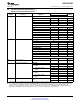
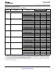
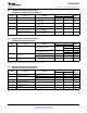
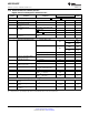
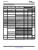
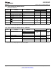
Specifications


ADC12D1800RF
SNAS518I –JULY 2011–REVISED JANUARY 2014
www.ti.com
Converter Electrical Characteristics
AC Electrical Characteristics (continued)
ADC12D1800RF
Units
Symbol Parameter Conditions
(Limits)
Typ Lim
Data Clock (DCLKI, DCLKQ)
DCLK Duty Cycle See
(1)
45 % (min)
50
55 % (max)
t
SR
Setup Time DCLK_RST± See
(2)
45 ps
t
HR
Hold Time DCLK_RST± See
(2)
45 ps
t
PWR
Pulse Width DCLK_RST± See
(1)
Sampling
Clock
5
Cycles
(min)
t
SYNC_DLY
DCLK Synchronization Delay 90° Mode
(1)
4 Sampling
Clock
0° Mode
(1)
5
Cycles
t
LHT
Differential Low-to-High Transition 10%-to-90%, C
L
= 2.5 pF
(2)
200 ps
Time
t
HLT
Differential High-to-Low Transition 10%-to-90%, C
L
= 2.5 pF
(2)
200 ps
Time
t
SU
Data-to-DCLK Setup Time 90° Mode
(1)
430 ps
t
H
DCLK-to-Data Hold Time 90° Mode
(1)
430 ps
t
OSK
DCLK-to-Data Output Skew 50% of DCLK transition to 50% of
±50 ps
Data transition
(1)
Data Input-to-Output
t
AD
Aperture Delay
(2)
Sampling CLK+ Rise to Acquisition
1.29 ns
of Data
t
AJ
Aperture Jitter See
(2)
0.2 ps (rms)
t
OD
Sampling Clock-to Data Output 50% of Sampling Clock transition
3.2 ns
Delay (in addition to Latency) to 50% of Data transition
(2)
t
LAT
Latency in 1:2 Demux Non-DES DI, DQ Outputs 34
Mode
(1)
DId, DQd Outputs 35
Latency in 1:4 Demux DES DI Outputs 34
Mode
(1)
DQ Outputs 34.5
Sampling
DId Outputs 35
Clock
DQd Outputs 35.5
Cycles
Latency in Non-Demux Non-DES DI Outputs 34
Mode
(1)
DQ Outputs 34
Latency in Non-Demux DES DI Outputs 34
Mode
(1)
DQ Outputs 34.5
t
ORR
Over Range Recovery Time Differential V
IN
step from ±1.2V to Sampling
0V to accurate conversion
(2)
1 Clock
Cycle
t
WU
Wake-Up Time (PDI/PDQ low to Non-DES Mode
(1)
500 ns
Rated Accuracy Conversion)
DES Mode
(1)
1 µs
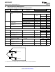
(1) This parameter is specified by design and is not tested in production.
(2) This parameter is specified by design and/or characterization and is not tested in production.
28 Electrical Specifications Copyright © 2011–2014, Texas Instruments Incorporated
Submit Documentation Feedback
Product Folder Links: ADC12D1800RF