
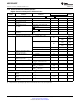
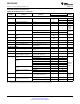
Specifications


V
D
+
V
D
-
V
OS
GND
½×V
OD
= | V
D
+ - V
D
- |
½×V
OD
V
D
-
V
D
+
ADC12D1800RF
SNAS518I –JULY 2011–REVISED JANUARY 2014
www.ti.com
4 Specification Definitions
APERTURE JITTER (t
AJ
) is the variation in aperture delay from sample-to-sample. Aperture jitter can be
effectively considered as noise at the input.
CODE ERROR RATE (CER) is the probability of error and is defined as the probable number of word
errors on the ADC output per unit of time divided by the number of words seen in that amount of time. A
CER of 10
-18
corresponds to a statistical error in one word about every 31.7 years.
CLOCK DUTY CYCLE is the ratio of the time that the clock waveform is at a logic high to the total time of
one clock period.
DIFFERENTIAL NON-LINEARITY (DNL) is the measure of the maximum deviation from the ideal step
size of 1 LSB. It is measured at the relevant sample rate, f
CLK
, with f
IN
= 1MHz sine wave.
EFFECTIVE NUMBER OF BITS (ENOB, or EFFECTIVE BITS) is another method of specifying Signal-to-
Noise and Distortion Ratio, or SINAD. ENOB is defined as (SINAD − 1.76) / 6.02 and states that the
converter is equivalent to a perfect ADC of this many (ENOB) number of bits.
GAIN ERROR is the deviation from the ideal slope of the transfer function. It can be calculated from Offset
and Full-Scale Errors. The Positive Gain Error is the Offset Error minus the Positive Full-Scale Error. The
Negative Gain Error is the Negative Full-Scale Error minus the Offset Error. The Gain Error is the
Negative Full-Scale Error minus the Positive Full-Scale Error; it is also equal to the Positive Gain Error
plus the Negative Gain Error.
GAIN FLATNESS is the measure of the variation in gain over the specified bandwidth. For example, for
the ADC12D1800RF, from D.C. to Fs/2 is to 900 MHz for the Non-DES Mode and from D.C. to Fs/2 is
1800 MHz for the DES Mode.
INTEGRAL NON-LINEARITY (INL) is a measure of worst case deviation of the ADC transfer function
from an ideal straight line drawn through the ADC transfer function. The deviation of any given code from
this straight line is measured from the center of that code value step. The best fit method is used.
INSERTION LOSS is the loss in power of a signal due to the insertion of a device, e.g. the
ADC12D1800RF, expressed in dB.
INTERMODULATION DISTORTION (IMD) is a measure of the near-in 3rd order distortion products (2f
2
-
f
1
, 2f
1
- f
2
) which occur when two tones which are close in frequency (f
1
, f
2
) are applied to the ADC input. It
is measured from the input tones level to the higher of the two distortion products (dBc) or simply the level
of the higher of the two distortion products (dBFS). The input tones are typically -7dBFS.
LSB (LEAST SIGNIFICANT BIT) is the bit that has the smallest value or weight of all bits. This value is
V
FS
/ 2
N
(1)
where V
FS
is the differential full-scale amplitude V
IN_FSR
as set by the FSR input and "N" is the ADC
resolution in bits, which is 12 for the ADC12D1800RF.
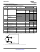
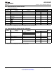
LOW VOLTAGE DIFFERENTIAL SIGNALING (LVDS) DIFFERENTIAL OUTPUT VOLTAGE (V
ID
and
V
OD
) is two times the absolute value of the difference between the V
D
+ and V
D
- signals; each signal
measured with respect to Ground. V
OD
peak is V
OD,P
= (V
D
+ - V
D
-) and V
OD
peak-to-peak is V
OD,P-P
=
2*(V
D
+ - V
D
-); for this product, the V
OD
is measured peak-to-peak.
Figure 4-1. LVDS Output Signal Levels
30 Specification Definitions Copyright © 2011–2014, Texas Instruments Incorporated
Submit Documentation Feedback
Product Folder Links: ADC12D1800RF