
Specifications


ADC12D1800RF
www.ti.com
SNAS518I –JULY 2011–REVISED JANUARY 2014
6 Functional Description
The ADC12D1800RF is a versatile A/D converter with an innovative architecture which permits very high
speed operation. The controls available ease the application of the device to circuit solutions. Optimum
performance requires adherence to the provisions discussed here and in the Applications Information
section. This section covers an overview, a description of control modes (Extended Control Mode and
Non-Extended Control Mode), and features.
6.1 OVERVIEW
The ADC12D1800RF uses a calibrated folding and interpolating architecture that achieves a high Effective
Number of Bits (ENOB). The use of folding amplifiers greatly reduces the number of comparators and
power consumption. Interpolation reduces the number of front-end amplifiers required, minimizing the load
on the input signal and further reducing power requirements. In addition to correcting other non-idealities,
on-chip calibration reduces the INL bow often seen with folding architectures. The result is an extremely
fast, high performance, low power converter.
The analog input signal (which is within the converter's input voltage range) is digitized to twelve bits at
speeds of 150 MSPS to 3.6 GSPS, typical. Differential input voltages below negative full-scale will cause
the output word to consist of all zeroes. Differential input voltages above positive full-scale will cause the
output word to consist of all ones. Either of these conditions at the I- or Q-input will cause the Out-of-
Range I-channel or Q-channel output (ORI or ORQ), respectively, to output a logic-high signal.
In ECM, an expanded feature set is available via the Serial Interface. The ADC12D1800RF builds upon
previous architectures, introducing a new DES Mode Timing Adjust, AutoSync feature for multi-chip
synchronization and increasing to 15-bit for gain and 12-bit plus sign for offset the independent
programmable adjustment for each channel.
Each channel has a selectable output demultiplexer which feeds two LVDS buses. If the 1:2 Demux Mode
is selected, the output data rate is reduced to half the input sample rate on each bus. When Non-Demux
Mode is selected, the output data rate on each channel is at the same rate as the input sample clock and
only one 12-bit bus per channel is active.
6.2 CONTROL MODES
The ADC12D1800RF may be operated in one of two control modes: Non-extended Control Mode (Non-
ECM) or Extended Control Mode (ECM). In the simpler Non-ECM (also sometimes referred to as Pin
Control Mode), the user affects available configuration and control of the device through the control pins.
The ECM provides additional configuration and control options through a serial interface and a set of 16
registers, most of which are available to the customer.
6.2.1 Non-Extended Control Mode
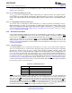
In Non-extended Control Mode (Non-ECM), the Serial Interface is not active and all available functions are
controlled via various pin settings. Non-ECM is selected by setting the ECE Pin to logic-high. Note that, for
the control pins, "logic-high" and "logic-low" refer to V
A
and GND, respectively. Nine dedicated control pins
provide a wide range of control for the ADC12D1800RF and facilitate its operation. These control pins
provide DES Mode selection, Demux Mode selection, DDR Phase selection, execute Calibration,
Calibration Delay setting, Power Down I-channel, Power Down Q-channel, Test Pattern Mode selection,
and Full-Scale Input Range selection. In addition to this, two dual-purpose control pins provide for AC/DC-
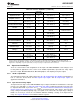
coupled Mode selection and LVDS output common-mode voltage selection. See Table 6-1 for a summary.
Copyright © 2011–2014, Texas Instruments Incorporated Functional Description 41
Submit Documentation Feedback
Product Folder Links: ADC12D1800RF