
Specifications

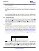


SDI
SDO
R/W
1 0 A3 A2 A1 A0 X
D14 D13 D12 D11 D10 D9 D8 D7 D6 D5 D4 D3 D2 D1 D0D15
21 43 65 87 109 1211 1413 1615 1817 2019 2221 2423 25
*Only required to be tri-stated in 3-wire mode.
SCLK
SCSb
ADC12D1800RF
www.ti.com
SNAS518I –JULY 2011–REVISED JANUARY 2014
SCLK: This signal is used to register the input data (SDI) on the rising edge; and to source the output
data (SDO) on the falling edge. The user may disable the clock and hold it at logic-low. There is no
minimum frequency requirement for SCLK; see f
SCLK
in Converter Electrical Characteristics Serial Port
Interface for more details.
SDI: Each register access requires a specific 24-bit pattern at this input, consisting of a command field
and a data field. If the SDI and SDO wired are shared (3-wire mode), then during read operations it is
necessary to tri-state the master which is driving SDI while the data field is being output by the ADC on
SDO. The master must be at TRI-STATE before the falling edge of the 8th clock. If SDI and SDO are not
shared (4-wire mode), then this is not necessary. Setup and hold times, t
SH
and t
SSU
, with respect to the
SCLK must be observed.
SDO: This output is normally at TRI-STATE and is driven only when SCS is asserted, the first 8 bits of
command data have been received and it is a READ operation. The data is shifted out, MSB first, starting
with the 8th clock's falling edge. At the end of the access, when SCS is de-asserted, this output is at TRI-
STATE once again. If an invalid address is accessed, the data sourced will consist of all zeroes. If it is a
read operation, there will be a bus turnaround time, t
BSU
, from when the last bit of the command field was
read in until the first bit of the data field is written out.
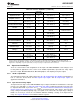
Table 6-3 shows the Serial Interface bit definitions.
Table 6-3. Command and Data Field Definitions
(1)
Bit No. Name Comments
1b indicates a read operation
1 Read / Write (R/W)
0b indicates a write operation
2-3 Reserved Bits must be set to 10b
16 registers may be addressed.
4-7 A<3:0>
The order is MSB first
8 X This is a "don't care" bit
Data written to or read from
9-24 D<15:0>
addressed register
(1) The serial data protocol is shown for a read and write operation in Figure 6-1 and Figure 6-2,
respectively.
Figure 6-1. Serial Data Protocol - Read Operation
Copyright © 2011–2014, Texas Instruments Incorporated Functional Description 45
Submit Documentation Feedback
Product Folder Links: ADC12D1800RF