
Specifications

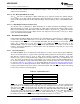

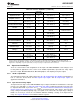


SDI
SDO
R/W
1 0 A3 A2 A1 A0 X D15 D14 D13 D12 D11 D10 D9 D8 D7 D6 D5 D4 D3 D2 D1 D0
21 43 65 87 109 1211 1413 1615 1817 2019 2221 2423 25
SCLK
SCSb
ADC12D1800RF
SNAS518I –JULY 2011–REVISED JANUARY 2014
www.ti.com
Figure 6-2. Serial Data Protocol - Write Operation
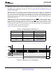
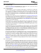
6.3 FEATURES
The ADC12D1800RF offers many features to make the device convenient to use in a wide variety of
applications. Table 6-4 is a summary of the features available, as well as details for the control mode
chosen. "N/A" means "Not Applicable."
Table 6-4. Features and Modes
Control Pin
Feature Non-ECM ECM Default ECM State
Active in ECM
Input Control and Adjust
AC/DC-coupled Mode Selected via V
CMO
Yes Not available N/A
Selection (Pin C2)
Selected via FSR Selected via the Config Reg
Input Full-scale Range Adjust No Low FSR value
(Pin Y3) (Addr: 3h and Bh)
Selected via the Config Reg
Input Offset Adjust Setting Not available N/A Offset = 0 mV
(Addr: 2h and Ah)
Selected via DES Selected via the DES Bit
DES/Non-DES Mode Selection No Non-DES Mode
(Pin V5) (Addr: 0h; Bit: 7)
Selected via the DCK Bit
DES Mode Input Selection Not available N/A N/A
(Addr: Eh; Bit: 6)
Selected via the DES Timing
DESCLKIQ Mode
(1)
Not available N/A Adjust Reg N/A
(Addr: 7h)
Selected via the DES Timing
DES Timing Adjust Not available N/A Mid skew offset
Adjust Reg (Addr: 7h)
Sampling Clock Phase Selected via the Config Reg
Not available N/A t
AD
adjust disabled
Adjust
(2)
(Addr: Ch and Dh)
Output Control and Adjust
Selected via DDRPh Selected via the DPS Bit
DDR Clock Phase Selection No 0° Mode
(Pin W4) (Addr: 0h; Bit: 14)
Selected via the SDR Bit
DDR / SDR DCLK Selection Not available N/A DDR Mode
(Addr: 0h; Bit: 2)
SDR Rising / Falling DCLK Selected via the DPS Bit
Not available N/A N/A
Selection
(1)
(Addr: 0h; Bit: 14)
(1) The -3 dB point is the traditional Full-Power Bandwidth (FPBW) specification. Although the insertion loss is approximately half the power
at this frequency, the dynamic performance of the ADC does not necessarily begin to degrade to a level below which it may be
effectively used in an application. The ADC may be used at input frequencies above the -3 dB FPBW point, for example, into the 3rd
Nyquist zone. Depending on system requirements, it is only necessary to compensate for the insertion loss.
(2) Sampling Clock Phase Adjust cannot be used in DES mode (DESI, DESQ, DESIQ or DESCLKIQ) at CLK frequencies above 1600 MHz.
46 Functional Description Copyright © 2011–2014, Texas Instruments Incorporated
Submit Documentation Feedback
Product Folder Links: ADC12D1800RF