
Specifications


Data
DCLK
0° Mode
DCLK
90° Mode
ADC12D1800RF
www.ti.com
SNAS518I –JULY 2011–REVISED JANUARY 2014
6.3.1.6 Sampling Clock Phase (Aperture) Delay Adjust
NOTE
Sampling Clock Phase Adjust cannot be used in DES mode (DESI, DESQ, DESIQ or
DESCLKIQ) at CLK frequencies above 1600 MHz.
The sampling clock (CLK) phase may be delayed internally to the ADC up to 825 ps in ECM. This feature
is intended to help the system designer remove small imbalances in clock distribution traces at the board
level when multiple ADCs are used, or to simplify complex system functions such as beam steering for
phase array antennas.
Additional delay in the clock path also creates additional jitter when using the sampling clock phase adjust.
Because the sampling clock phase adjust delays all clocks, including the DCLKs and output data, the user
is strongly advised to use the minimal amount of adjustment and verify the net benefit of this feature in his
system before relying on it.
Using this feature at its maximum setting, for the maximum sampling clock rate, may affect the integrity of
the sampling clock on chip. Therefore, it is not recommended to do so. The maximum setting for the
coarse adjust is 825ps. The period for the maximum sampling clock rate of is 555ps, so it should not be
necessary to exceed this value in any case.
6.3.2 Output Control and Adjust
There are several features and configurations for the output of the ADC12D1800RF so that it may be used
in many different applications. This section covers DDR clock phase, LVDS output differential and
common-mode voltage, output formatting, Demux/Non-demux Mode, Test Pattern Mode, and Time Stamp.
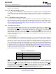
6.3.2.1 SDR / DDR Clock
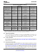
The ADC12D1800RF output data can be delivered in Double Data Rate (DDR) or Single Data Rate
(SDR). For DDR, the DCLK frequency is half the data rate and data is sent to the outputs on both edges
of DCLK; see Figure 6-3. The DCLK-to-Data phase relationship may be either 0° or 90°. For 0° Mode, the
Data transitions on each edge of the DCLK. Any offset from this timing is t
OSK
; see Converter Electrical
Characteristics AC Electrical Characteristics for details. For 90° Mode, the DCLK transitions in the middle
of each Data cell. Setup and hold times for this transition, t
SU
and t
H
, may also be found in Converter
Electrical Characteristics AC Electrical Characteristics. The DCLK-to-Data phase relationship may be
selected via the DDRPh Pin in Non-ECM (see Dual Data Rate Phase Pin (DDRPh)) or the DPS bit in the
Configuration Register (Addr: 0h; Bit: 14) in ECM. Note that for Non-Demux Mode, 90° DDR Mode is not
available.
Figure 6-3. DDR DCLK-to-Data Phase Relationship
Copyright © 2011–2014, Texas Instruments Incorporated Functional Description 49
Submit Documentation Feedback
Product Folder Links: ADC12D1800RF