
Specifications


ADC12D1800RF
SNAS518I –JULY 2011–REVISED JANUARY 2014
www.ti.com
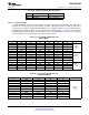
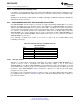
Table 6-7. Test Pattern by Output Port in
Non-Demux Mode (continued)
Time Q I ORQ ORI Comments
T10 000h 004h 0b 0b
T11 000h 004h 0b 0b
Pattern
T12 FFFh FFBh 1b 1b Sequence
n+1
T13 FFFh FFBh 1b 1b
T14 ... ... ... ...
6.3.2.7 Time Stamp
The Time Stamp feature enables the user to capture the timing of an external trigger event, relative to the
sampled signal. When enabled via the TSE Bit (Addr: 0h; Bit: 3), the LSB of the digital outputs (DQd, DQ,
DId, DI) captures the trigger information. In effect, the 12-bit converter becomes an 11-bit converter and
the LSB acts as a 1-bit converter with the same latency as the 11-bit converter. The trigger should be
applied to the DCLK_RST input. It may be asynchronous to the ADC sampling clock.
6.3.3 Calibration Feature
The ADC12D1800RF calibration must be run to achieve specified performance. The calibration procedure
is exactly the same regardless of how it was initiated or when it is run. Calibration trims the analog input
differential termination resistors, the CLK input resistor, and sets internal bias currents which affect the
linearity of the converter. This minimizes full-scale error, offset error, DNL and INL, which results in the
maximum dynamic performance, as measured by: SNR, THD, SINAD (SNDR) and ENOB.
6.3.3.1 Calibration Control Pins and Bits
Table 6-8 is a summary of the pins and bits used for calibration. See Ball Descriptions and Equivalent
Circuits for complete pin information and Figure 4-8 for the timing diagram.
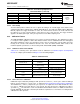
Table 6-8. Calibration Pins
Pin (Bit) Name Function
D6 CAL
Initiate calibration
(Addr: 0h; Bit 15) (Calibration)
CalDly
V4 Select power-on calibration delay
(Calibration Delay)
(Addr: 4h) Calibration Adjust Adjust calibration sequence
CalRun Indicates while calibration is
B5
(Calibration Running) running
Rtrim+/- External resistor used to calibrate
C1/D2
(Input termination trim resistor) analog and CLK inputs
Rext+/- External resistor used to calibrate
C3/D3
(External Reference resistor) internal linearity
6.3.3.2 How to Execute a Calibration
Calibration may be initiated by holding the CAL pin low for at least t
CAL_L
clock cycles, and then holding it
high for at least another t
CAL_H
clock cycles, as defined in Converter Electrical Characteristics Calibration.
The minimum t
CAL_L
and t
CAL_H
input clock cycle sequences are required to ensure that random noise does
not cause a calibration to begin when it is not desired. The time taken by the calibration procedure is
specified as t
CAL
. The CAL Pin is active in both ECM and Non-ECM. However, in ECM, the CAL Pin is
logically OR'd with the CAL Bit, so both the pin and bit are required to be set low before executing another
calibration via either pin or bit.
52 Functional Description Copyright © 2011–2014, Texas Instruments Incorporated
Submit Documentation Feedback
Product Folder Links: ADC12D1800RF