
Specifications


ADC12D1800RF
SNAS518I –JULY 2011–REVISED JANUARY 2014
www.ti.com
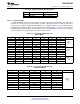
In the case that only one channel is used in Non-DES Mode or that the ADC is driven in DESI or DESQ
Mode, the unused analog input should be terminated to reduce any noise coupling into the ADC. See
Table 6-9 for details.
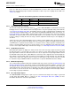
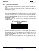
Table 6-9. Unused Analog Input Recommended Termination
Mode Power Down Coupling Recommended Termination
Non-DES Yes AC/DC Tie Unused+ and Unused- to Vbg
DES/Non-DES No DC Tie Unused+ and Unused- to Vbg
DES/Non-DES No AC Tie Unused+ to Unused-
6.4.1.3 FSR and the Reference Voltage
The full-scale analog differential input range (V
IN_FSR
) of the ADC12D1800RF is derived from an internal
bandgap reference. In Non-ECM, this full-scale range must be set by the logic-high setting of the FSR Pin;
see Full-Scale Input Range Pin (FSR). The FSR Pin operates on both I- and Q-channels. In ECM, the full-
scale range may be independently set for each channel via Addr:3h and Bh with 15 bits of precision; see
Register Definitions. The best SNR is obtained with a higher full-scale input range, but better distortion
and SFDR are obtained with a lower full-scale input range. It is not possible to use an external analog
reference voltage to modify the full-scale range, and this adjustment should only be done digitally, as
described.
A buffered version of the internal bandgap reference voltage is made available at the V
BG
Pin for the user.
The V
BG
pin can drive a load of up to 80 pF and source or sink up to 100 μA. It should be buffered if more
current than this is required. This pin remains as a constant reference voltage regardless of what full-scale
range is selected and may be used for a system reference. V
BG
is a dual-purpose pin and it may also be
used to select a higher LVDS output common-mode voltage; see LVDS Output Common-mode Pin (VBG).
6.4.1.4 Out-Of-Range Indication
Differential input signals are digitized to 12 bits, based on the full-scale range. Signal excursions beyond
the full-scale range, i.e. greater than +V
IN_FSR
/2 or less than -V
IN_FSR
/2, will be clipped at the output. An
input signal which is above the FSR will result in all 1's at the output and an input signal which is below
the FSR will result in all 0's at the output. When the conversion result is clipped for the I-channel input, the
Out-of-Range I-channel (ORI) output is activated such that ORI+ goes high and ORI- goes low while the
signal is out of range. This output is active as long as accurate data on either or both of the buses would
be outside the range of 000h to FFFh. The Q-channel has a separate ORQ which functions similarly.
6.4.1.5 Maximum Input Range
The recommended operating and absolute maximum input range may be found in Operating Ratings and
Absolute Maximum Ratings, respectively. Under the stated allowed operating conditions, each Vin+ and
Vin- input pin may be operated in the range from 0V to 2.15V if the input is a continuous 100% duty cycle
signal and from 0V to 2.5V if the input is a 10% duty cycle signal. The absolute maximum input range for
Vin+ and Vin- is from -0.15V to 2.5V. These limits apply only for input signals for which the input common
mode voltage is properly maintained.
6.4.1.6 AC-coupled Input Signals
The ADC12D1800RF analog inputs require a precise common-mode voltage. This voltage is generated
on-chip when AC-coupling Mode is selected. See AC / DC-Coupled Mode Pin (VCMO) for more
information about how to select AC-coupled Mode.
56 Functional Description Copyright © 2011–2014, Texas Instruments Incorporated
Submit Documentation Feedback
Product Folder Links: ADC12D1800RF