
Specifications


ADC12D1XXX
V
IN
+
50:
Source
V
IN
-
1:2 Balun
C
couple
C
couple
100:
V
IN
+
V
IN
-
V
CMO
ADC12D1XXX
C
couple
C
couple
ADC12D1800RF
www.ti.com
SNAS518I –JULY 2011–REVISED JANUARY 2014
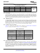
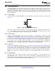
In AC-coupled Mode, the analog inputs must of course be AC-coupled. For an ADC12D1800RF used in a
typical application, this may be accomplished by on-board capacitors, as shown in Figure 6-6. For the
ADC12D1800RFRB, the SMA inputs on the Reference Board are directly connected to the analog inputs
on the ADC12D1800RF, so this may be accomplished by DC blocks (included with the hardware kit).
When the AC-coupled Mode is selected, an analog input channel that is not used (e.g. in DES Mode)
should be connected to AC ground, e.g. through capacitors to ground . Do not connect an unused analog
input directly to ground.
Figure 6-6. AC-coupled Differential Input
The analog inputs for the ADC12D1800RF are internally buffered, which simplifies the task of driving
these inputs and the RC pole which is generally used at sampling ADC inputs is not required. If the user
desires to place an amplifier circuit before the ADC, care should be taken to choose an amplifier with
adequate noise and distortion performance, and adequate gain at the frequencies used for the application.
6.4.1.7 DC-coupled Input Signals
In DC-coupled Mode, the ADC12D1800RF differential inputs must have the correct common-mode
voltage. This voltage is provided by the device itself at the V
CMO
output pin. It is recommended to use this
voltage because the V
CMO
output potential will change with temperature and the common-mode voltage of
the driving device should track this change. Full-scale distortion performance falls off as the input common
mode voltage deviates from V
CMO
. Therefore, it is recommended to keep the input common-mode voltage
within 100 mV of V
CMO
(typical), although this range may be extended to ±150 mV (maximum). See V
CMI
in Converter Electrical Characteristics Analog Input / Output and Reference Characteristics and ENOB vs.
V
CMI
in Typical Performance Plots. Performance in AC- and DC-coupled Mode are similar, provided that
the input common mode voltage at both analog inputs remains within 100 mV of V
CMO
.
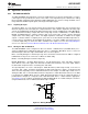
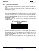
6.4.1.8 Single-Ended Input Signals
The analog inputs of the ADC12D1800RF are not designed to accept single-ended signals. The best way
to handle single-ended signals is to first convert them to differential signals before presenting them to the
ADC. The easiest way to accomplish single-ended to differential signal conversion is with an appropriate
balun-transformer, as shown in Figure 6-7.
Figure 6-7. Single-Ended to Differential Conversion Using a Balun
When selecting a balun, it is important to understand the input architecture of the ADC. The impedance of
the analog source should be matched to the ADC12D1800RF's on-chip 100Ω differential input termination
resistor. The range of this termination resistor is specified as R
IN
in Converter Electrical Characteristics
Analog Input / Output and Reference Characteristics.
Copyright © 2011–2014, Texas Instruments Incorporated Functional Description 57
Submit Documentation Feedback
Product Folder Links: ADC12D1800RF