
Specifications


CLK+
CLK-
ADC12D1XXX
C
couple
C
couple
ADC12D1800RF
SNAS518I –JULY 2011–REVISED JANUARY 2014
www.ti.com
6.4.2 THE CLOCK INPUTS
The ADC12D1800RF has a differential clock input, CLK+ and CLK-, which must be driven with an AC-
coupled, differential clock signal. This provides the level shifting necessary to allow for the clock to be
driven with LVDS, PECL, LVPECL, or CML levels. The clock inputs are internally terminated to 100Ω
differential and self-biased. This section covers coupling, frequency range, level, duty-cycle, jitter, and
layout considerations.
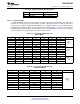
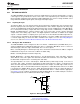
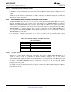
6.4.2.1 CLK Coupling
The clock inputs of the ADC12D1800RF must be capacitively coupled to the clock pins as indicated in
Figure 6-8.
Figure 6-8. Differential Input Clock Connection
The choice of capacitor value will depend on the clock frequency, capacitor component characteristics and
other system economic factors. For example, on the ADC12D1800RFRB, the capacitors have the value
C
couple
= 4.7 nF which yields a high pass cutoff frequency, f
c
= 677.2 kHz.
6.4.2.2 CLK Frequency
Although the ADC12D1800RF is tested and its performance is ensured with a differential 1.8 GHz
sampling clock, it will typically function well over the input clock frequency range; see f
CLK
(min) and
f
CLK
(max) in Converter Electrical Characteristics AC Electrical Characteristics. Operation up to f
CLK
(max) is
possible if the maximum ambient temperatures indicated are not exceeded. Operating at sample rates
above f
CLK
(max) for the maximum ambient temperature may result in reduced device reliability and
product lifetime. This is due to the fact that higher sample rates results in higher power consumption and
die temperatures. If f
CLK
< 300 MHz, enable LFS in the Control Register (Addr: 0h, Bit 8).
6.4.2.3 CLK Level
The input clock amplitude is specified as V
IN_CLK
in Converter Electrical Characteristics Sampling Clock
Characteristics. Input clock amplitudes above the max V
IN_CLK
may result in increased input offset voltage.
This would cause the converter to produce an output code other than the expected 2047/2048 when both
input pins are at the same potential. Insufficient input clock levels will result in poor dynamic performance.
Both of these results may be avoided by keeping the clock input amplitude within the specified limits of
V
IN_CLK
.
6.4.2.4 CLK Duty Cycle
The duty cycle of the input clock signal can affect the performance of any A/D converter. The
ADC12D1800RF features a duty cycle clock correction circuit which can maintain performance over the
20%-to-80% specified clock duty-cycle range. This feature is enabled by default and provides improved
ADC clocking, especially in the Dual-Edge Sampling (DES) Mode.
58 Functional Description Copyright © 2011–2014, Texas Instruments Incorporated
Submit Documentation Feedback
Product Folder Links: ADC12D1800RF