
Specifications


ADC12D1800RF
SNAS518I –JULY 2011–REVISED JANUARY 2014
www.ti.com
6.4.5 SUPPLY / GROUNDING, LAYOUT AND THERMAL RECOMMENDATIONS
6.4.5.1 Power Planes
All supply buses for the ADC should be sourced from a common linear voltage regulator. This ensures
that all power buses to the ADC are turned on and off simultaneously. This single source will be split into
individual sections of the power plane, with individual decoupling and connection to the different power
supply buses of the ADC. Due to the low voltage but relatively high supply current requirement, the
optimal solution may be to use a switching regulator to provide an intermediate low voltage, which is then
regulated down to the final ADC supply voltage by a linear regulator. Please refer to the documentation
provided for the ADC12D1800RFRB for additional details on specific regulators that are recommended for
this configuration.
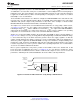
Power for the ADC should be provided through a broad plane which is located on one layer adjacent to
the ground plane(s). Placing the power and ground planes on adjacent layers will provide low impedance
decoupling of the ADC supplies, especially at higher frequencies. The output of a linear regulator should
feed into the power plane through a low impedance multi-via connection. The power plane should be split
into individual power peninsulas near the ADC. Each peninsula should feed a particular power bus on the
ADC, with decoupling for that power bus connecting the peninsula to the ground plane near each power /
ground pin pair. Using this technique can be difficult on many printed circuit CAD tools. To work around
this, zero ohm resistors can be used to connect the power source net to the individual nets for the different
ADC power buses. As a final step, the zero ohm resistors can be removed and the plane and peninsulas
can be connected manually after all other error checking is completed.
6.4.5.2 Bypass Capacitors
The general recommendation is to have one 100nF capacitor for each power / ground pin pair. The
capacitors should be surface mount multi-layer ceramic chip capacitors similar to Panasonic part number
ECJ-0EB1A104K.
6.4.5.3 Ground Planes
Grounding should be done using continuous full ground planes to minimize the impedance for all ground
return paths, and provide the shortest possible image/return path for all signal traces.
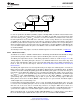
6.4.5.4 Power System Example
The ADC12D1800RFRB uses continuous ground planes (except where clear areas are needed to provide
appropriate impedance management for specific signals), see Figure 6-10. Power is provided on one
plane, with the 1.9V ADC supply being split into multiple zones or peninsulas for the specific power buses
of the ADC. Decoupling capacitors are connected between these power bus peninsulas and the adjacent
ground planes using vias. The capacitors are located as close to the individual power / ground pin pairs of
the ADC as possible. In most cases, this means the capacitors are located on the opposite side of the
PCB to the ADC.
62 Functional Description Copyright © 2011–2014, Texas Instruments Incorporated
Submit Documentation Feedback
Product Folder Links: ADC12D1800RF