
Specifications


ADC12D1800RF
SNAS518I –JULY 2011–REVISED JANUARY 2014
www.ti.com
The center ground balls should be soldered down to the recommended ball pads (See AN-1126). These
balls will have wide traces which in turn have vias which connect to the internal ground planes, and a
bottom ground pad / pour if possible. This ensures a good ground is provided for these balls, and that the
optimal heat transfer will occur between these balls and the PCB ground planes.
In spite of these package enhancements, analysis using the standard JEDEC JESD51-7 four-layer PCB
thermal model shows that ambient temperatures must be limited to a max of 65°C to ensure a safe
operating junction temperature for the ADC12D1800RF. However, most applications using the
ADC12D1800RF will have a printed circuit board which is more complex than that used in JESD51-7.
Typical circuit boards will have more layers than the JESD51-7 (eight or more), several of which will be
used for ground and power planes. In those applications, the thermal resistance parameters of the
ADC12D1800RF and the circuit board can be used to determine the actual safe ambient operating
temperature up to a maximum of 85°C.
Three key parameters are provided to allow for modeling and calculations. Because there are two main
thermal paths between the ADC die and external environment, the thermal resistance for each of these
paths is provided. θ
JC1
represents the thermal resistance between the die and the exposed metal area on
the top of the HSBGA package. θ
JC2
represents the thermal resistance between the die and the center
group of balls on the bottom of the HSBGA package. The final parameter is the allowed maximum junction
temperature, which is T
J
.
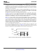
In other applications, a heat sink or other thermally conductive path can be added to the top of the
HSBGA package to remove heat. In those cases, θ
JC1
can be used along with the thermal parameters for
the heat sink or other thermal coupling added. Representative heat sinks which might be used with the
ADC12D1800RF include the Cool Innovations p/n 3-1212XXG and similar products from other vendors. In
many applications, the printed circuit board will provide the primary thermal path conducting heat away
from the ADC package. In those cases, θ
JC2
can be used in conjunction with printed circuit board thermal
modeling software to determine the allowed operating conditions that will maintain the die temperature
below the maximum allowable limit. Additional dissipation can be achieved by coupling a heat sink to the
copper pour area on the bottom side of the printed circuit board.
Typically, dissipation will occur through one predominant thermal path. In these cases, the following
calculations can be used to determine the maximum safe ambient operating temperature:
T
J
= T
A
+ P
D
× (θ
JC
+θ
CA
)
T
J
= T
A
+ P
C(MAX)
× (θ
JC
+θ
CA
)
For θ
JC
, the value for the primary thermal path in the given application environment should be used (θ
JC1
or θ
JC2
). θ
CA
is the thermal resistance from the case to ambient, which would typically be that of the heat
sink used. Using this relationship and the desired ambient temperature, the required heat sink thermal
resistance can be found. Alternately, the heat sink thermal resistance can be used to find the maximum
ambient temperature. For more complex systems, thermal modeling software can be used to evaluate the
printed circuit board system and determine the expected junction temperature given the total system
dissipation and ambient temperature.
6.4.6 SYSTEM POWER-ON CONSIDERATIONS
There are a couple important topics to consider associated with the system power-on event including
configuration and calibration, and the Data Clock.
6.4.6.1 Power-on, Configuration, and Calibration
Following the application of power to the ADC12D1800RF, several events must take place before the
output from the ADC12D1800RF is valid and at full performance; at least one full calibration must be
executed with the device configured in the desired mode.
64 Functional Description Copyright © 2011–2014, Texas Instruments Incorporated
Submit Documentation Feedback
Product Folder Links: ADC12D1800RF