
Specifications


Power-on
Calibration
On-command
Calibration
Power to
ADC
Calibration
CalDly
Pull-up/down
resistors set
Control Pins
ADC output
valid
ADC12D1800RF
www.ti.com
SNAS518I –JULY 2011–REVISED JANUARY 2014
Following the application of power to the ADC12D1800RF, there is a delay of t
CalDly
and then the Power-
on Calibration is executed. This is why it is recommended to set the CalDly Pin via an external pull-up or
pull-down resistor. This ensured that the state of that input will be properly set at the same time that power
is applied to the ADC and t
CalDly
will be a known quantity. For the purpose of this section, it is assumed
that CalDly is set as recommended.
The Control Bits or Pins must be set or written to configure the ADC12D1800RF in the desired mode. This
must take place via either Extended Control Mode or Non-ECM (Pin Control Mode) before subsequent
calibrations will yield an output at full performance in that mode. Some examples of modes include
DES/Non-DES Mode, Demux/Non-demux Mode, and Full-Scale Range.
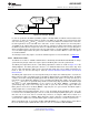
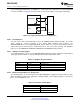
The simplest case is when device is in Non-ECM and the Control Pins are set by pull-up / down resistors,
see Figure 6-12. For this case, the settings to the Control Pins ramp concurrently to the ADC voltage.
Following the delay of t
CalDly
and the calibration execution time, t
CAL
, the output of the ADC12D1800RF is
valid and at full performance. If it takes longer than t
CalDly
for the system to stabilize at its operating
temperature, it is recommended to execute an on-command calibration at that time.
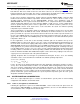
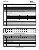
Another case is when the FPGA configures the Control Pins (Non-ECM) or writes to the SPI (ECM), see
Figure 6-13. It is always necessary to comply with the Operating Ratings and Absolute Maximum ratings,
i.e. the Control Pins may not be driven below the ground or above the supply, regardless of what the
voltage currently applied to the supply is. Therefore, it is not recommended to write to the Control Pins or
SPI before power is applied to the ADC12D1800RF. As long as the FPGA has completed writing to the
Control Pins or SPI, the Power-on Calibration will result in a valid output at full performance. Once again,
if it takes longer than t
CalDly
for the system to stabilize at its operating temperature, it is recommended to
execute an on-command calibration at that time.
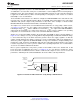
Due to system requirements, it may not be possible for the FPGA to write to the Control Pins or SPI
before the Power-on Calibration takes place, see Figure 6-14. It is not critical to configure the device
before the Power-on Calibration, but it is critical to realize that the output for such a case is not at its full
performance. Following an On-command Calibration, the device will be at its full performance.
Figure 6-12. Power-on with Control Pins set by Pull-up / down Resistors
Copyright © 2011–2014, Texas Instruments Incorporated Functional Description 65
Submit Documentation Feedback
Product Folder Links: ADC12D1800RF