
Specifications


ADC12D1800RF
www.ti.com
SNAS518I –JULY 2011–REVISED JANUARY 2014
6.5 Register Definitions
Twelve read / write registers provide several control and configuration options in the Extended Control
Mode. These registers have no effect when the device is in the Non-extended Control Mode. Each register
description below also shows the Power-On Reset (POR) state of each control bit. See Table 6-14 for a
summary. For a description of the functionality and timing to read / write the control registers, see The
Serial Interface.
NOTE
Register 6h must be written to 1C0Eh for the device to perform at full rated performance for
Fclk > 1.6GHz.
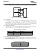
Table 6-14. Register Addresses
A3 A2 A1 A0 Hex Register Addressed
0 0 0 0 0h Configuration Register 1
0 0 0 1 1h Reserved
0 0 1 0 2h I-channel Offset
0 0 1 1 3h I-channel Full-Scale Range
0 1 0 0 4h Calibration Adjust
0 1 0 1 5h Calibration Values
0 1 1 0 6h Bias Adjust
0 1 1 1 7h DES Timing Adjust
1 0 0 0 8h Reserved
1 0 0 1 9h Reserved
1 0 1 0 Ah Q-channel Offset
1 0 1 1 Bh Q-channel Full-Scale Range
1 1 0 0 Ch Aperture Delay Coarse Adjust
1 1 0 1 Dh Aperture Delay Fine Adjust
1 1 1 0 Eh AutoSync
1 1 1 1 Fh Reserved
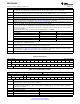
Table 6-15. Configuration Register 1
Addr: 0h (0000b) POR state: 2000h
Bit 15 14 13 12 11 10 9 8 7 6 5 4 3 2 1 0
Name CAL DPS OVS TPM PDI PDQ Res LFS DES DEQ DIQ 2SC TSE SDR Res
POR 0 0 1 0 0 0 0 0 0 0 0 0 0 0 0 0
Bit 15 CAL: Calibration Enable. When this bit is set to 1b, an on-command calibration is initiated. This bit is not reset automatically
upon completion of the calibration. Therefore, the user must reset this bit to 0b and then set it to 1b again to execute another
calibration. This bit is logically OR'd with the CAL Pin; both bit and pin must be set to 0b before either is used to execute a
calibration.
(1)
Bit 14 DPS: DCLK Phase Select. In DDR Mode, set this bit to 0b to select the 0° Mode DDR Data-to-DCLK phase relationship and to
1b to select the 90° Mode. In SDR Mode, set this bit to 0b to transition the data on the Rising edge of DCLK; set this bit to 1b
to transition the data on the Falling edge of DCLK.
Bit 13 OVS: Output Voltage Select. This bit sets the differential voltage level for the LVDS outputs including Data, OR, and DCLK. 0b
selects the lower level and 1b selects the higher level. See V
OD
in Converter Electrical Characteristics Digital Control and
Output Pin Characteristics for details.
Bit 12 TPM: Test Pattern Mode. When this bit is set to 1b, the device will continually output a fixed digital pattern at the digital Data
and OR outputs. When set to 0b, the device will continually output the converted signal, which was present at the analog
inputs. See Test Pattern Mode for details about the TPM pattern.
(1) This pin / bit functionality is not tested in production test; performance is tested in the specified / default mode only.
Copyright © 2011–2014, Texas Instruments Incorporated Functional Description 69
Submit Documentation Feedback
Product Folder Links: ADC12D1800RF