
Specifications


ADC12D1800RF
www.ti.com
SNAS518I –JULY 2011–REVISED JANUARY 2014
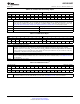
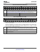
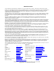
Table 6-26. Q-channel Full-Scale Range Adjust
Addr: Bh (1011b) POR state: 4000h
Bit 15 14 13 12 11 10 9 8 7 6 5 4 3 2 1 0
Name Res FM(14:0)
POR 0 1 0 0 0 0 0 0 0 0 0 0 0 0 0 0
Bit 15 Reserved. Must be set to 0b.
Bits 14:0 FM(14:0): FSR Magnitude. These bits increase the ADC full-scale range magnitude (straight binary coding.) The allowable
range is from 800 mV (16384d) to 1000 mV (32767d) with the default setting at 800 mV (16384d). Monotonicity is specified by
design only for the 9 MSBs. A greater range of FSR values is available in ECM, i.e. FSR values above 800 mV. See V
IN_FSR
in
Converter Electrical Characteristics Analog Input / Output and Reference Characteristics for characterization details.
Code FSR [mV]
100 0000 0000 0000 (default) 800
111 1111 1111 1111 1000
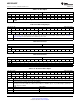
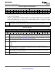
Table 6-27. Aperture Delay Coarse Adjust
Addr: Ch (1100b) POR state: 0004h
Bit 15 14 13 12 11 10 9 8 7 6 5 4 3 2 1 0
Name CAM(11:0) STA DCC Res
POR 0 0 0 0 0 0 0 0 0 0 0 0 0 1 0 0
Aperture Delay Adjust feature cannot be used in DES mode (DESI, DESQ, DESIQ or DESCLKIQ) for CLK
frequencies above 1600 MHz.
Using the t
AD
Adjust feature at its maximum setting, for the maximum sampling clock rate, may affect the
integrity of the sampling clock on chip. Therefore, it is not recommended to do so. The maximum setting
for the coarse adjust is 825ps. The period for the maximum sampling clock rate of is 555ps, so it should
not be necessary to exceed this value in any case.
Bits 15:4 CAM(11:0): Coarse Adjust Magnitude. This 12-bit value determines the amount of delay that will be applied to the input CLK
signal. The range is 0 ps delay for CAM(11:0) = 0d to a maximum delay of 825 ps for CAM(11:0) = 2431d (±95 ps due to PVT
variation) in steps of ~340 fs. For code CAM(11:0) = 2432d and above, the delay saturates and the maximum delay applies.
Additional, finer delay steps are available in register Dh. The STA (Bit 3) must be selected to enable this function.
Bit 3 STA: Select t
AD
Adjust. Set this bit to 1b to enable the t
AD
adjust feature, which will make both coarse and fine adjustment
settings, i.e. CAM(11:0) and FAM(5:0), available.
Bit 2 DCC: Duty Cycle Correct. This bit can be set to 0b to disable the automatic duty-cycle stabilizer feature of the chip. This
feature is enabled by default.
Bits 1:0 Reserved. Must be set to 0b.
Copyright © 2011–2014, Texas Instruments Incorporated Functional Description 73
Submit Documentation Feedback
Product Folder Links: ADC12D1800RF