EV10AQ190x-DK VITA 57 FMC Quad 10-bit ADC Demo Kit
EV10AQ190x-DK User Guide 1067BX–BDC–12/11
Table of Contents Section 1 General Overview ................................................................................. 1-1 1.1 1.2 1.3 Disclaimer .................................................................................................1-1 Quad 10-bit ADC.......................................................................................1-2 Demo Kit ...................................................................................................1-3 Section 2 Quick Start ..............
.5.3 Input Impedance...............................................................................4-22 4.5.4 CLOCK .............................................................................................4-24 4.5.5 Power ...............................................................................................4-25 4.5.6 Acquisition Control............................................................................4-26 4.5.7 Acquisition ....................................................
General Overview Section 1 General Overview The QUAD 10-bit Demo Kit enables the easy evaluation of the characteristics and performance of QUAD 10-bit ADC EV10AQ190x. The Demo kit is plug_and_play and needs little external equipment. The Demo kit is delivered with software which allows acquisition of data using the FPGA. The QUAD 10-bit Demo Kit is compatible with VITA57 FMC (FPGA Mezzanine Card) standard. For more information please see the VITA site web. http://www.vita.com/fmc.
General Overview This kit must be regarded as a tool, not a finished product. It allows the evaluation of performance of the e2v component, design prototypes and debug software. It CANNOT be resold as a finished product that must be compliant with local relevant regulations. Its function is as a development system, demonstrating the performance of e2v semiconductors components and not as a final product available on general release.
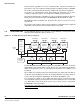
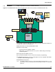
General Overview 1.3 Demo Kit Figure 1-2 provides an overview of system architecture. Figure 1-2. EV10AQ190x-DK Demo Kit System Architecture (when Connected with a VIRTEX6 Evaluation Kit) 12V supply adapter RF generator CLK DN D C B A PC GUI control, acquisition & analysis I/O USB control 4 channels e2v QUAD 10-bit VITA57 interface FPGA 12V supply adapter (VIRTEX 6) The complete system is built with the e2v demo kit and an FPGA development kit.
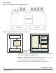
General Overview Figure 1-3. EV10AQ190x-DK Demo Kit Simplified Schematic Figure 1-4. EV10AQ190x-DK Demo Kit Functional Architecture Device PC ADC Control & Events FPGA Acquisition & formatting Display Processing Acquisition FX2 USB Transport Layer USB cable Driver USB USB Transport Layer USB Acquisition and formatting of ADC digital output data are done within the FPGA Eval Kit. Data is then transmitted again to the ADC Demo Kit.
Quick Start Section 2 Quick Start 2.1 Operating Procedure 1. Install the Software as described in section 4 Software Tools. 2. Install the FPGA code into ML605 Xilinx evaluation board (see Section 5.3 “FPGA Programming” ) 3. Turn OFF the ML605 Xilinx evaluation board. 4. Fix Heatsink/Fan to the ADC if no external form of ventilation is to be used (see Section 3.4) 5. Connect the QUAD 10-bit Demo Kit on ML605 Xilinx evaluation board. 6. Connect the power supplies of both evaluation boards. 7.
Quick Start Figure 2-1. USB Port Driver Configuration Warning: this installation is done for one USB connector only. If USB connector is changed, USB driver need to be re-installed before use. 2.2.2 Start up Procedure Check that supplies are properly powered on and properly connected. Check if the Xilinx FPGA evaluation board ML605 is properly configured with correct software. Check if QUAD 10-bit Demo Kit is properly plugged into FPGA connector. Check if USB connector is properly plugged. 2.
Quick Start Figure 2-2. FFT without Windowing or with non Coherent Signal Figure 2-3. FFT with Windowing Warning: if the Fin frequency has an exact value such as 250 MHz the FTT result is wrong that is why it is recommended to perform measurements with shift of few MHz e.g. 250.2 MHz.
Quick Start Figure 2-4. Example of Wrong INL Measurement if Incorrect Fin such as Exactly 250 MHz With channel A and channel C (amplifier channels) an RF attenuator should be added on the SMA connecter to have optimum performance. When these channels are not being used the attenuator or 50 Ohm terminator should be kept in place. This will prevent the amplifiers from adding noise into the system. Figure 2-5.
Quick Start Check if acquisition is synchronous. The ADC RAMP test procedure will set the ADC to output a ramp on each channel these ramps are synchronous at the output of the ADC after a SYNC process has been completed. The FPGA RESET done during this procedure will always ensure that the 4 channels are acquired in the FPGA synchronously. However if the channels are found not to be synchronous as shown in Figure 2-7. Figure 2-7.
Quick Start Figure 2-8. Synchronous Channels Note: 2.3 External Equipment it is not always necessary to have the ramp patterns aligned to obtain correct data acquisition using the analog inputs. Even if the ramp mode is not synchronous, you could return to the normal mode and perform one acquisition. Normally the acquisition of sinus wave in normal mode is correct. The QUAD 10-bit Demo Kit needs very little external hardware.
Quick Start Option RF generator for clock input signal whose frequency is different than 2 GHz – The QUAD 10-bit Demo Kit provides clock signal at 2 GHz using its own PLL – The QUAD 10-bit Demo Kit could be tested with other clock frequency Please see Section 6.2 Clock selection Table 2-1.
Quick Start 2-8 1067BX–BDC–12/11 e2v semiconductors SAS 2011 EV10AQ190x-DK - User Guide
Main Functions Section 3 Main Functions 3.1 Analog Input Signal The user only needs to provide an analog signal at the input. This signal is digitized by the ADC depending on the chosen operating mode: 4 channel mode (1 channel per ADC core) 2 channel mode (2 interleaved ADC cores) 1 channel mode (4 interleaved ADC cores) Each channel input is driven in different ways on the board: Single to Differential Amplifier from Analog Devices (A channel: ADA4960 D.C.
Main Functions Figure 3-1. Analog Input SMA Configuration A channel 3.1.1 Analog Input Channel A B channel C channel D channel Ext Clock The Analog input channel A uses a differential amplifier (ADC driver) from Analog Devices ref: ADA4960. Figure 3-2.
Main Functions The ADA4960 is used in DC configuration with output common mode driven by ADC QUAD 10-bit. The input is biased at 2.5V since this is a requirement for best performance from the amplifier, this should be taken into account when using this input. Note: be careful that if a DC voltage is added after the RF generator output that this will not damage the generator. The ADA4960 is used in AC configuration in channel C. 3.1.
Main Functions 3.1.4 Analog Input Channel D This channel is free for customer use in differential and AC coupling configuration. Figure 3-5. Channel D : Schematic This Channel D could be used in DC configuration. Please see Section 6.1Channel D. 3.2 ADC Clock Input Signal ADC clock input is generated by Clock generated PLL Hititte HMC831 (on-board) at 2.0 GHz. This frequency is fixed. Figure 3-6.
Main Functions 3.3 Control of ADC Settings The Graphical User Interface allows for complete monitoring and control of all the settings of EV10AQ190x Quad 10-bit ADC such as channel selection, Gain, Offset, Phase, test mode (with SPI signal). Please see Section 4.5 Operating Modes. Please refer to datasheet EV10AQ190x for more information. http://www.e2v.
Main Functions In other applications with the component positioned differently a simple heatsink (4°C/W max) will be sufficient. Thermal analysis should be performed on any proposed arrangement. Figure 3-8. Position of Heat Sink/fan 3.5 ADC Current Consumption Monitoring The ADC currents (ICC, ICCO and ICCD) can be measured by the Demo Kit. Figure 3-9. ADC Measurement (Partial): Schematic ADC currents (ICC, ICCO and ICCD) can also be monitored via the GUI. Please see Section 4.5.5 Power.
Main Functions 3.6 ADC SYNC Signal The QUAD 10-bit ADC requires a SYNC signal when the internal configuration is changed (for example Channel configuration, DMUX configuration, test mode ….). The QUAD 10-bit Demo Kit performs this SYNC signal automatically when these modes are changed. The SYNC signal is driven by microcontroller FX2 and the D950LV0011 devices transform the single ended signal into an LVDS signal. Figure 3-10.
Main Functions Figure 3-11. 3V3A Power Supplies Figure 3-12. 1.8V Power Supplies The amplifier and PLL power supply uses low noise LDO regulators from Linear Technology.
Main Functions Figure 3-13.
Main Functions 3-10 1067BX–BDC–12/11 e2v semiconductors SAS 2011 EV10AQ190x-DK - User Guide
Software Tools Section 4 Software Tools 4.1 Overview The Demo Kit board needs three different kinds of software tools: FPGA software The Demo Kit board can be plugged with XILINX VIRTEX 6 evaluation board EK-V6ML605-G http://www.xilinx.com/products/devkits/EK-V6-ML605-G.htm e2v provides FPGA program to be used with Quad 10-bit Demo Kit.
Software Tools 4.2 Configuration The advised configuration for Windows 2000/98/XP and Windows NT is: "PC with Intel Pentium Microprocessor of over 100 MHz; "Memory of at least 24 Mo. For other versions of Windows OS, use the recommended configuration from Microsoft. 4.3 User Interface Installation 1. Install the Quad 10-bit Demo Kit application on your computer by launching the SetupEvalkitQuadAdc10Bits.exe installer (please refer to the latest version available).
Software Tools 2. Select Destination Directory Figure 4-3. Quad 10-bit Demo Kit Application "Select Destination Directory" 3. Select Components (Start Menu Folder) Figure 4-4.
Software Tools 4. Select Components (Additional Tasks) Figure 4-5. Quad 10-bit Demo Kit Application "Additional Tasks" 5. Select Components (Ready to Install) Figure 4-6.
Software Tools If you agree with the install configuration, press Install button. Now a new process of installation started Processing&Display for installing Labview RunTime (no license required. Please follow instructions. Warning: don't press finish button on "Completing Setup wizard" window. The screen shown in Figure 4-7 is displayed: 6. Select Components Processing&Display (installation Wizard) Figure 4-7.
Software Tools 7. Select Components Processing&Display (Destination Folder) Figure 4-8. Quad 10-bit Demo Kit Processing&Display "Destination Folder" 8. Select Components Processing&Display (Install the Application) Figure 4-9. Quad 10-bit Demo Kit Processing&Display "Install the Application" The installation of the software is now completed but the Processing&Display software need to be launched. This installation is launched automatically.
Software Tools 9. Select Components Processing&Display (Completing Setup wizard" window) Figure 4-10. Quad 10-bit Demo Kit Processing&Display "Completing Setup Wizard" Window" 10. Select Quad 10-bit Demo Kit application (Completing Setup wizard" window) Figure 4-11. Quad 10-bit Demo Kit Application "Completing Setup Wizard" Window" Note about README message. Please follow instruction before using Quad 10-bit Demo Kit application.
Software Tools Figure 4-12. README Message For the bugs/limitation for Excel display, please see Section 4.5.10 Regional and Language Options. 4.4 USB Driver Installation After the installation, Quad 10-bit Demo Kit can be powered up and connected to PC with USB cable. At the first connection a USB driver installation will be launched. Warning: if the Demo Kit is connected to another USB connector this installation must be re-started. The installation is normally fully automatic.
Software Tools Figure 4-14. Allow Windows to Search Driver Please choose: Yes, always search online (recommended) Figure 4-15.
Software Tools Figure 4-16. Choose the Folder Select C:\Program Files\E2V\EvalkitQuadAdc10Bits Figure 4-17. Warning: Installation Please choose: Install the driver software anyway A Data transfer has been beginning please wait.
Software Tools Figure 4-18. END of New Driver Installation The new driver has been installed After the installation, the interface can be launched with the following file: C:\Program Files\E2V\EvalkitQuadAdc10Bits\EvalkitQuadAdc10Bits.
Software Tools The window shown in Figure 4-19 will be displayed. Figure 4-19.
Software Tools 4.5 Operating Modes The Quad 10-bit ADC software included with the Demo Kit provides a Graphical User Interface to configure the ADC. Push buttons, popup menus and capture windows allows easy: 1. Settings; 2. Test; 3. Gain / Offset / Phase; 4. Input Impedance; 5. Clock; 6. Power; 7. Acquisition; With Setting, Test, Clock and Acquisition windows always click on "APPLY" button to validate any command. Clicking the "CANCEL" button will restore last settings sent with "APPLY" button.
Software Tools Figure 4-24. Demo Kit User Interface with Hide Tab Configuration On the bottom corner the software displays information about software and hardware revision. ChipId: revision of Quad 10-bit ADC Device: revision of FX2 software FPGA: revision of VHDL code Figure 4-25.
Software Tools 4.5.1 Settings Figure 4-26.
Software Tools ADC mode: 4-channels mode = the 4 ADCs work independently at Fclock/2 sampling rate (where Fclock is the external clock signal frequency). Figure 4-27. ADC Mode: 4-channels Mode 2-channels mode = the 4 ADCs are interleaved 2 by 2 (A & B, C & D), the sampling rate is equal to Fclock (where Fclock is the external clock signal frequency), the analog inputs can be applied to A or B and respectively C or D. Figure 4-28.
Software Tools Figure 4-29. ADC Mode: 1-channel Mode Simultaneous channel mode = the analog input signal of channel A or B or C or D is sent to the 4 ADCs work at the same clock (4 ADC with the same timing) with Fclock/2 sampling rate (where Fclock is the external clock signal frequency). Figure 4-30. ADC Mode: Simultaneous Sampling General setting: Output mode = Gray coding or Binary coding Bandwidth selection: Nominal give 1.5 GHz bandwidth at -3dB; Full gives 3.
Software Tools Standby setting: No standby = all channels are active (A: ON, B: ON, C: ON, D: ON); Partial standby = either A & B are in standby or C & D are in standby; Full standby = all 4 ADCs are in standby. Figure 4-31. Standby Configuration Synchronization: Synchronization: programs the number of clock cycles prior to output clock restart after SYNC reset Figure 4-32.
Software Tools 4.5.2 TEST In this window, the test mode is available: A ramp test is generated within each ADC and output Figure 4-34. Test Ramp Test Mode Note: this mode allows synchronizing the 4 channels of ADC with the FPGA RESET. The synchronizing procedure can be initiated by checking the Disable button and then the Apply button : Then check the ADC and Ramp button and then Apply. Then retrun to normal operation by checking the Disable button and clicking on Apply.
Software Tools Figure 4-36. FPGA Test Mode Gain / Offset / Phase Figure 4-37. Gain / Offset / Phase Settings In this window, it is possible to adjust gain, offset and phase of the selected channel via the "channel select" button on the top left of the user interface.
Software Tools A LED shows if the channel is ON (active - green LED) or OFF (not active - red LED) and if the same channel is ready (ready to receive gain, offset or phase orders - green LED) or busy (not ready to receive new calibration orders - red LED). Figure 4-38.
Software Tools Figure 4-40. Gain Write Send Sequence 4.5.3 Input Impedance 4-22 1067BX–BDC–12/11 e2v semiconductors SAS 2011 Figure 4-41.
Software Tools In this window, it is possible to re-adjust the internal input resistor, which should be matched to 50. The procedure is similar to the previous ones: select the channel where you need to adjust the input impedance check that the channel is ON and READY (green LEDs) enter the resistor value push the WRITE button to write these values to the internal registers (you can retrieve the initial value of the impedance by clicking on the CANCEL button) Figure 4-42.
Software Tools 4.5.4 CLOCK This sheet allows selection between the Internal PLL or external clock. Figure 4-43. User Interface Demo Kit - Clock Settings Note: because of limitation of ML605 evaluation board (LVDS max 1GHz in speed grade -1). The capture of Quad 10-bit data is limited to 2 GSps.
Software Tools 4.5.5 Power This sheet allows measurement of the Quad 10-bit power consumption and the internal junction temperature. Figure 4-44.
Software Tools 4.5.6 Acquisition Control This sheet controls the acquisition modes of the Quad 10-bit. Figure 4-45.
Software Tools Sampling Nbr: Number of samples in acquisition Must be a 2n For FFT N=4X2n (n=number bit of ADC). For INL N=16X2n (n=number bit of ADC) Example for 10-bit ADC FFT must be computed with 4096 points and INL with 16384 points Nb Harmonics: Number of Harmonics considered for THD and SNR calculation (Default value is 10 harmonics). FFT window: When the analog input signal and the sampling clock are not coherent signals, a FFT windows has to be applied to obtain a correct result.
Software Tools Select directory Figure 4-48. Directory Selection Note: 4.5.7 Acquisition A manual operation is needed to name and save the file. The stream function can be used to start an acquisition Snap: for single acquisition Start for continuous acquisition, (stop acquisition with the stop button) Figure 4-49.
Software Tools Figure 4-50. Sample Signal: Example of Signal in Simultaneous Channel Figure 4-51.
Software Tools Figure 4-52. FFT Spectrum Example Figure 4-53.
Software Tools Plot selection: one channel or several channels can be plotted for easier reading. Figure 4-54. Plot Selection Figure 4-55. Zoom Selection: Several Kinds of Zoom can be chosen Figure 4-56.
Software Tools Figure 4-57. Cursor Selection: and Move Cursor on Channel FFT parameters: this channel selection has to be used to see FFT parameters of several channels Selection 0 => ADC Channel A Selection 1 => ADC Channel B Selection 2 => ADC Channel C Selection 3 => ADC Channel D Figure 4-58.
Software Tools FFT Processing: For future calculations, we define: N Sig = Signal power level = ""spectrumi 2 0 setup.PeakWidth Ho = Power of the continuous component = spectrum i 2 0 setup.PeakWidth H1 = Power of the fundamental = spectrumi 2 j setup.cal..Nbr of Harmonics ""setup.
Software Tools SINAD dBFS = -10 log 10 (-SNR dBFS/ /10) + 10 (THD dBFS/ /10) SINAD dBFS – 10 log 1.5 ENOB dBFS = --------------------------------------------------------------6.02 The parameters with the _FS prefix correspond to the same parameter but in dBFS (from full scale). 4.5.8 Demo Kit Configuration File It is possible to save the context of the Demo Kit (saving of all settings and configuration). This context can be saved for later use, so that saved settings can be reloaded.
Software Tools 4.5.9 Data Save File It is also possible to save the data of your acquisition (saving of all data samples and FFT result).
Software Tools 4.5.10 Regional and Language Options Use a control Regional Setting to check if decimal separator is configured with a dot ".". Figure 4-61.
Software Tools Selection: Customize this format. Figure 4-62. Customize Regional Option Sheet Numbers The decimal separator must be configured with a dot ".
Software Tools 4-38 1067BX–BDC–12/11 e2v semiconductors SAS 2011 EV10AQ190x-DK - User Guide
FPGA CODE Section 5 FPGA CODE The FPGA code has been designed to be used with ML605 Xilinx Virtex 6 evaluation board. Figure 5-1. ML605 Xilinx® VIRTEX® 6 Evaluation Board Warning: Please configure your ML605 evaluation board with correct Switch configuration. 5.1 Software Configuration 5.
FPGA CODE 5.3 FPGA Programming Connect the USB Mini cable on USB JTAG connector J22 Change the Configuration Mode Switch and System ACE Address Figure 5-2. Configuration Mode Switch of ML 605 Board Launch the iMPACT of ISE suite and load the CDROM\FPGA bin\bin\prog_q10.ipf Figure 5-3. Loading of DKQUAD10bit.ipf file Note: ensure that program into PROM is correctly programmed. Don't forget to program the CDROM\FPGA Bin\progQ10_V1.1.mcs file into PROM.
FPGA CODE Figure 5-4. Programming the File PROM\DKQUAD10bit.mcs Figure 5-5.
FPGA CODE 5.4 VHDL CODE A documentation of VHDL architecture is provided with the Demo Kit. See CDROM\Documentation\FPGA Code\ DK_QUAD10_bits_FPGA_Design_Document_v1.pdf Figure 5-6.
Demo kit Hardware Configuration Section 6 Demo kit Hardware Configuration The Demo Kit could be hardware configured by changing manually some capacitor or resistance. This chapter describes all user settable hardware configurations. 6.1 Channel D The Channel D could be used in DC configuration mode by replacing C126 and C127 by a 0 resistor. Figure 6-1. Channel D Schematic 6.2 Clock Selection The ADC clock is generated by a PLL, but an external clock can be used (for frequency different than PLL).
Demo kit Hardware Configuration Figure 6-2. ADC Clock Selection Schematic Figure 6-3. Implantation of R15, R37, R36 and R50 Resistors TOP VIEW 6.3 SPI Signal The SPI signal is controlled by the FX2 microcontroller, but it could also be controlled by FPGA. The selection between the two clocks is done manually with a resistor. Note: e2v doesn't provide the SPI controller FPGA code. Remove R93, R95, R97, R99 and R101 resistors and solder R94, R96, R98, R100 and R102 with a 0.
Demo kit Hardware Configuration Figure 6-4. SPI Schematic Figure 6-5.
Demo kit Hardware Configuration 6.4 SYNC Signal The SYNC signal is controlled by the FX2 microcontroller, but it could also be controlled by the FPGA. The selection between the two clocks is done manually with a resistor. Note: e2v doesn't provide the SYNC signal FPGA code. Remove R105 resistor and solder R106 with a 0. Figure 6-6. SYNC Schematic Figure 6-7.
Layout Information Section 7 Layout Information Figure 7-1. Top Side Layer 1 Figure 7-2.
Layout Information 7-2 1067AX–BDC–06/11 e2v semiconductors SAS 2011 EV10AQ190x-DK - User Guide
Mechanical Dimensions Section 8 Mechanical Dimensions The Demo Kit board with Quad 10-bit ADC dimension is 139 mm × 76.5 mm × 8 mm. It is compatible with VITA57 FMC standard. Figure 8-1.
Mechanical Dimensions 8-2 1067AX–BDC–06/11 e2v semiconductors SAS 2011 EV10AQ190x-DK - User Guide
Ordering Information Section 9 Ordering Information Table 9-1.
Ordering Information 9-2 1067BX–BDC–12/11 e2v semiconductors SAS 2011 EV10AQ190x-DK - User Guide
How to reach us Home page: www.e2v.com Sales offices: Europe Regional sales office Americas e2v ltd e2v inc 106 Waterhouse Lane 520 White Plains Road Chelmsford Essex CM1 2QU Suite 450 Tarrytown, NY 10591 England USA Tel: +44 (0)1245 493493 Tel: +1 (914) 592 6050 or 1-800-342-5338, Fax: +44 (0)1245 492492 Fax: +1 (914) 592-5148 mailto: enquiries@e2v.com mailto: enquiries-na@e2v.com e2v sas Asia Pacific 16 Burospace e2v ltd F-91572 Bièvres Cedex 11/F.
1067BX–BDC–12/11 e2v semiconductors SAS 2011