
User`s guide

Registers • 17
3.1 I/O Port Base Address
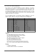
The registers of the cPCI/PCI-7300A are shown in Table 3.1. The base
address of these registers is als o assigned by the PCI P&P BIOS. The
assigned base address is stored at offset 18h of the PCR. Therefore, users
can read the PCR to know the base address by using BIOS function call. Note
that the cPCI/PCI-7300A registers are all 32 bits. Users should access these
registers by 32 bits I/O instructions.
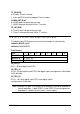
The PCI-7300A occupies 8 consecutive 32-bit I/O addresses in the I/O
address space. Table 3.1 shows the I/O Map of the PCI-7300A rev.B.
Address Read Write
Base + 0 DI_CSR DI_CSR
Base + 4 DO_CSR DO_CSR
Base + 8 AUX_DIO AUX_DIO
Base + C INT_CSR INT_CSR
Base + 10 DI_FIFO DI_FIFO
Base + 14 DO_FIFO DO_FIFO
Base + 18 - FIFO_CR
Base + 1C POL_CTRL POL_CTRL
Base + 20 8254_COUNT0 8254_COUNT0
Base + 24 8254_COUNT1 8254_COUNT1
Base + 28 8254_COUNT2 8254_COUNT2
Base + 2C
8254_CONTROL 8254_CONTROL
Legend:
DI_CSR: Digital input control & status register
DO_SCR: Digital output control & status register
AUX_DIO: Auxiliary digital I/O port
INT_CSR: Interrupt control and status register
DI_FIFO: DI FIFO direct access port
DO_FIFO: DO FIFO direct access port
FIFO_CR: FIFO almost empty/full programming register
POL_CTRL: Polarity control register for the control signals
Caution:
1. I/O port is 32-bit width
2. 8-bit or 16-bit I/O access is not allowed.