cPCI-9116®/cPCI-9116R® 64 Ch, 16 bit, 250KS/s Analog input Card For 3U CompactPCI User’s Guide Recycled Paper
Copyright 2002 ADLINK Technology Inc. All Rights Reserved. Manual Rev. 1.02: JUL 23, 2002 Part No: 50-15002-100 The information in this document is subject to change without prior notice in order to improve reliability, design and function and does not represent a commitment on the part of the manufacturer.
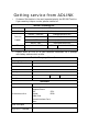
Getting service from ADLINK • Customer Satisfaction is the most important priority for ADLINK Tech Inc. If you need any help or service, please contact us. ADLINK Technology Inc. Web Site http://www.adlinktech.com Sales & Service Service@adlinktech.com NuDAQ + USBDAQ nudaq@adlinktech.com Technical Automation automation@adlinktech.com Support NuIPC nuipc@adlinktech.com TEL +886-2-82265877 NuPRO / EBC Address • nupro@adlinktech.com FAX +886-2-82265717 9F, No.
Table of Contents Tables .....................................................................................iii Figures .....................................................................................iv How to Use This Guide .............................................................v Chapter 1 Introduction..............................................................1 1.1 Features ............................................................................. 1 1.2 Applications ..................
4.6 Channel Gain Queue Register ........................................... 24 4.7 A/D & FIFO Control Register .............................................. 25 4.8 A/D & FIFO Status Register ............................................... 27 4.9 Digital I/O register ............................................................. 28 4.10 A/D Trigger Mode Register ................................................ 29 4.11 Interrupt Control Register................................................... 31 4.
Tables Table 1. Legend of J1 Connector ......................................... 14 Table 2. I/O Port Address .................................................... 19 Table 3. Timer/Counter Register Address............................. 20 Table 4. General Purpose Timer/Counter Register ................ 21 Table 5. General Purpose Timer/Counter Control Register .... 22 Table 6. GPTC0’s Mode selection........................................ 23 Table 7. A/D Data Registers ..........................
Figures Figure 1: PCB Layout of the cPCI-9116 ................................... 9 Figure 2: PCB Layout of cPCI-9116R and Rear I/O adaptor .... 10 Figure 3: J1 Pin Assignments ............................................... 13 Figure 4: Single-ended Mode and Floating sources ................ 15 Figure 5: Ground-referenced source and differential input....... 16 Figure 6: Floating source and differential input .......................
How to Use This Guide This manual is designed to help you use the 9116 series. The manual describes how to modify various settings on the card to meet your requirements. It is divided into seven chapters: Chapter1, “Introduction”, gives an overview of the product features, applications, and specifications. Chapter 2, “Installation”, describes how to install the 9116 series . The layout of 9116 series is shown.
1 Introduction The 9116 series products are advanced data acquisition cards based on the 32-bit CompactPCI architecture. The 9116 series include: • cPCI-9116 : 16-bit 250KHz DAS card for 3U CompactPCI • cPCI-9116R : 16-bit 250KHz DAS card for 3U CompactPCI with Rear I/O connector The 9116 series DAS cards use state-of-the-art technology making it an ideal for data logging and signal analysis applications in medical, process control, etc. 1.
• Five A/D trigger modes: software trigger, pre-trigger, post-trigger, middle-trigger and delay-trigger • Software Polling, Interrupt and Bus-mastering DMA data transfer available • 8 digital input and 8 digital o utput channels • 100-pin D-type SCSI-II connector for cPCI-9116 • 100-pin D-type SCSI-II connector on a rear I/O transition board for cPCI-9116R • Compact size: standard compact PCI 3U size 1.
1.3 ♦ Specifications Analog Input (A/D) • Converter: LT1606 (or equivalent) 250KHz • Number of channels: (programmable) P 64 single-ended (SE) P 32 differential input (DI) P Mixing of SE and DI analog signal between channel allowed • A/D Data FIFO Buffer Size: 1024 locations • Channel Gain Queue Length: 512 words configurations • Resolution: 16-bit • Input Range: (Controlled by Channel Gain Queue) • P Bipolar: ± 5V, ±2.5V, ±1.25V, ±0.625V P Unipolar: 0~10V, 0~5V, 0~2.5V, 0~1.
• • • ♦ ♦ P Software-trigger. P Pre-trigger. P Post-trigger. P Middle-Trigger. P Delay Trigger Data Transfer: P Polling. P EOC interrupt transfer. P FIFO half-full Interrupt transfer. P Bus-mastering DMA. Data Throughput: 250KHz (maximum) Digital I/O (DIO) • Channel: 8 TTL compatible digital inputs and outputs • Input Voltage: • ♦ Trigger Mode: P Low: VIL=0.8 V max. IIL=0.2mA max. P High: VIH=2.0V max. IIH=0.02mA max Output Voltage: P Low: VOL=0.5 V max. IOL=8mA max.
P +5V @ 560mA typical P +3.3V@ 100mA typical • ± 15V (pin35, pin85) Output Current (max): 5mA • +5V(pin49, pin99) Output Current (max): 500mA • Dimension: Standard Compact PCI 3U size 1.4 Software Support ADLINK provides versatile software drivers and packages for users’ different approach to building a system. We not only provide programming libraries such as DLL for many Windows systems, but also provide drivers for other software packages such as LabVIEW®.
1.4.2 ® PCIS-LVIEW: LabVIEW Driver PCIS-LVIEW contains the VIs, which are used to interface with NI’s LabVIEW® software package. The PCIS-LVIEW supports Windows 95/98/NT/2000. The LabVIEW® drivers is shipped free with the board. You can install and use them without a license. For more information about PCIS-LVIEW, please refer to the user’s guide in the CD. (\\Manual_PDF\Software\PCIS-LVIEW) 1.4.
2 Installation This chapter describes how to install the 9116 series cards. The contents of the package and unpacking information that you should be aware of are described first. The 9116 series cards perform an automatic configuration of the IRQ, port address, and BIOS address. You do not need to set these configurations, as you would do in ISA form factor DAS cards. Automatic configuration allows your system to operate more reliable and safe. 2.
2.2 Unpacking The card contains electro-static sensitive components that can be easily be damaged by static electricity. Therefore, the card should be handled on a grounded anti-static mat. The operator should be wearing an anti-static wristband, grounded at the same point as the anti-static mat. Inspect the card module carton for obvious damages. Shipping and handling may cause damage to your module. Be sure there are no shipping and handling damages on the modules carton before continuing.
2.
Figure 2: PCB Layout of cPCI-9116R and Rear I/O adaptor 10 • Installation
2.4 1. PCI Configuration Plug and Play: As a plug and play component, the board requests an interrupt number via a system call. The system BIOS responds with an interrupt assignment based on the board information and on known system parameters. These system parameters are determined by the installed drivers and the hardware load seen by the system. 2. Configuration: The board configuration is done on a board-by-board basis for all PCI form factor boards on your system.
3 Signal Connections This chapter describes the connectors of the 9116 series. The signal connections between the 9116 series cards and external devices are also outlined. 3.1 Connectors and Pin Assignment The cPCI-9116 is equipped with one 100-pin SCSI-type connector (J1). J1 is used for digital input/output, analog input, and timer/counter signals. The pin assignment for the connector is illustrated in the Figure 3.1.
J1 100-pin SCSI-type connector AIH0 AIH1 AIH2 AIH3 AIH4 AIH5 AIH6 AIH7 AIH8 AIH9 AIH10 AIH11 AIH12 AIH13 AIH14 AIH15 AIH16 AIH17 AIH18 AIH19 AIH20 AIH21 AIH22 AIH23 AIH24 AIH25 AIH26 AIH27 AIH28 AIH29 AIH30 AIH31 U_CMMD AI0 AI1 AI2 AI3 AI4 AI5 AI6 AI7 AI8 AI9 AI10 AI11 AI12 AI13 AI14 AI15 AI16 AI17 AI18 AI19 AI20 AI21 AI22 AI23 AI24 AI25 AI26 AI27 AI28 AI29 AI30 AI31 AGND +15V out N/C DI0 DI1 DI2 DI3 DI4 DI5 DI6 DI7 ExtTimeBase ExtTrg SSH_OUT GP_TC_OUT +5V Out DGND 1 2 3 4 5 6 7 8 9 10 11 12 13 14 15 16 1
Legend of J1: Signal Name Definition U_CMMD User Common Mode AIn Analog Input Channel n (single-ended) AIHn Analog High Input Channel n (differential) AILn Analog Low Input Channel n (differential) DIn Digital Input Signal Channel n DOn Digital Output Signal Channel n ExtTimeBase External Timebase Clock Input ExtTrg External Digital Trigger Signal SSH_OUT SSH Output Signal GP_TC_CLK General Purpose Timer/Counter Clock Input GP_TC_GATE General Purpose Timer/Counter Gate Input GP_TC_UP
3.2 Analog Input Signal Connection The 9116 series provides up to 64 single-ended or 32 differential analog input channels. You can set and fill the Channel Gain Queue to get the desired combination of the input signal types. The analog signals can be converted to digital value by the A/D converter.
Differential input mode The differential input mode provides two inputs that respond to signal voltage differences between them. If the signal source is ground- referenced, the differential mode can be used for common-mode noise rejection. Figure 5 shows the connection of ground-referenced signal sources under differential input mode. Input Multipexer x = 0, ...
User Common Mode (U_CMMD) To measure ground-referenced signal sources, which are connected to the same ground point, you can connect the signals in a User-Common-Mode (U_CMMD) configuration. Fig 7 illustrates the connections. The signal local ground reference is connected to the negative input of the instrumentation Amplifier, and the common-mode ground potential to signal ground. The instrumentation amplifier will now reject the 9116 series ground.
4 Registers The descriptions of the registers and structure of the PCI-9116 are outlined in this chapter. The information in this chapter will assist programmers, who wish to handle the card with low-level programs. In addition, the low level programming syntax is introduced. This information can help beginners to operate the PCI-9116 in the shortest possible time. 4.1 I/O Port Address The 9116 series card functions as a 32-bit PCI master device to any master on the PCI bus.
I/O Address Read Write Base + 0x00 Scan Interval Counter Scan Interval Counter Base + 0x04 Sample Interval Counter Sample Interval Counter Base + 0x08 Scan Counter Scan Counter Base + 0x0C DIV Counter DIV Counter Base + 0x10 Delay1 Counter Delay1 Counter Base + 0x14 M Counter M Counter Base + 0x18 GP Counter/Timer 0 GP Counter/Timer 0 Base + 0x1C X X Base + 0x20 X GP Counter/Timer Control Reg Base + 0x24 A/D FIFO Data Reg Config. Channel Gain Queue Reg..
4.2 Internal Timer/Counter Register The 9116 series card basically has 6 counters, which are responsible for the scan timing of the analog input data acquisition. The 6 counters occupy 6 I/O address locations in the 9116 card as shown below.
4.3 General Purpose Timer/Counter Register One 16-bit, general-purpose timer/counter exists in the 9116 series card. Writing to this register loads the initial count value into the general-purpose timer/counter.
4.4 General Purpose Timer/Counter Control Register Address: BASE + 0x20 Attribute: write only Data Format: Bit 7 6 5 4 3 Up Counter Up Clk_sr Down Gate_src en c Down src Bit Bit Bit 15 2 1 0 --- MODE1 MODE 0 14 13 12 11 10 9 8 --- --- --- --- --- --- --- 23 22 21 20 19 18 17 16 --- --- --- --- --- --- --- --- 31 30 29 28 27 26 25 24 --- --- --- --- --- --- --- --- Table 5.
Clk_src (bit3): GPTC0’s clock source 1: External Input (Pin 96) 0: Internal Timebase MODE1~MODE0 (bit1 ~ bit0): MODE1 MODE0 Description 0 0 General Counter 0 1 Pulse Generation 1 0 X 1 1 X Table 6. 4.5 GPTC0’s Mode selection GPTC0’s Mode selection A/D Data Registers The digital converted data is 16-bits and is stored into 32-bit registers.
4.6 Channel Gain Queue Register This register is used to fill the Channel Gain Queue. We recommend users use our call function to avoid any possible errors from these settings.
HL_sel(bit3): >31 channel selection (single ended) 1: when channel number is larger than 31 0: when channel number is smaller than or equal to 31 DIFF(bit1): Analog Input Signals Type 1: Differential 0: Single ended UNIP(bit2): Analog Input Signals Polarity 1: Unipolar 0: Bipolar U_CMMD (bit0): User Defined Common Mode Selection 1: User Defined Common Mode (Pin 1) 0: Local Ground of 9116 series 4.
DMA (Bit8): Write Only, set for DMA transfer SC_dis (Bit7): Write Only, set to disable the SC counter Clear Channel Gain Queue (Bit6): Write Only Clear the Channel Gain Queue 0: no effect on the Channel Gain Queue 1: clear the Channel Gain Queue Set done (Bit5): Write Only 0: indicate the Channel Gain Queue is not ready 1: indicate the Channel Gain Queue is OK Clear DFIFO(Bit4) : Write Only Clear the Data FIFO: 0: no effect on Data FIFO 1: clear the Data FIFO Clear Trg_det(Bit3) : Write 1 to clear Write 1 t
4.8 A/D & FIFO Status Register Address: BASE + 28 Attribute: read Data Format: Bit Bit Bit Bit 7 6 5 4 3 2 1 0 ACQ Full HFull Empty Trg_det SC_TC ADOR ADOS 15 14 13 12 11 10 9 8 --- --- --- --- --- --- --- --- 23 22 21 20 19 18 17 16 --- --- --- --- --- --- --- --- 31 30 29 28 27 26 25 24 --- --- --- --- --- --- --- --- Table 11. A/D & FIFO Status Register ACQ (Bit7): Read Only, set when acquisition is in progress.
SC_TC(Bit2) : Read/ Write 1 to clear Scan Counter Terminal Count Status 1: Scan Counter counts to 0 0: Scan Counter not completed ADOR(Bit1) : Read/ Write 1 to clear A/D Overrun Status (Fatal Error !) 1: A/D Overrun 0: A/D not Overrun ADOS(Bit0) : Read/ Write 1 to clear A/D Over Speed Status (Warning !) 1: A/D Over Speed 0: A/D not Over Speed 4.9 Digital I/O register There are 8 digital input and 8 digital output channels provided by the 9116 series cards.
Address: BASE + 30 Attribute: write Data Format: Bit 7 6 5 4 3 2 1 0 DO7 DO6 DO5 DO4 DO3 DO2 DO1 DO0 15 14 13 12 11 10 9 8 --- --- --- --- --- --- --- --- 23 22 21 20 19 18 17 16 --- --- --- --- --- --- --- --- 31 30 29 28 27 26 25 24 --- --- --- --- --- --- --- --- Bit Bit Bit Table 13. Digital I/O register (Write) 4.
softconv (bit10): ADC direct conversion control 1: generate 1 convert pulse 0: no effect ACQ_EN (bit9): Acquisition enable bit 1: enable the acquisition timing 0: disable the acquisition timing M_enable (bit8): M counter enable bit 1: ignore trigger signals before M counter reaches 0 0: accept the trigger signal anytime Retrig (bit7): Re-triggerability in an acquisition 1: Re-triggerable 0: trigger only once DLY SRC (bit6): Delay time unit in delay trigger mode 1: delay in sampling rate (SI2) 0: delay
4.11 Interrupt Control Register Address: BASE + 0x38 Attribute: write Data Format: Bit Bit Bit Bit 7 6 5 4 3 2 1 0 --- --- --- Clr_Timer Clr_STTC 15 14 13 12 11 10 --- --- --- Timer_en STTC_en Hfull_en 23 22 21 20 19 18 17 16 --- --- --- --- --- --- --- --- 31 30 29 28 27 26 25 24 --- --- --- --- --- --- --- --- Clr_Hfull Clr_DTrg Clr_EOC 9 8 DTrg_en EOC_en Table 16.
EOC_en (bit8): End of conversion Interrupt Enable Control 1: Enable 0: Disable Clr_Timer (bit4): write 1 to clear the GPTC Interrupt status 1: clear interrupt from the GPTC 0: no effect Clr_SCTC (bit3): write 1 to clear the SCTC Interrupt 1: clear the interrupt on terminal count of the Scan counter 0: no effect Clr_HFull (bit2): write 1 to clear the data FIFO half full interrupt 1: clear the interrupt on the data FIFO half full status 0: no effect Clr_DTrg (bit1): write 1 to clear the Digital Trigger Interr
4.12 Interrupt Status Register Address: BASE + 0x38 Attribute: read Data Format: Bit Bit Bit Bit 7 6 5 4 3 2 1 0 --- --- --- Timer STTC Hfull DTrg EOC 15 14 13 12 11 10 9 8 --- --- --- --- --- --- --- --- 23 22 21 20 19 18 17 16 --- --- --- --- --- --- --- --- 31 30 29 28 27 26 25 24 --- --- --- --- --- --- --- --- Table 17.
5 Operation Theory The operation theory of the functions on the 9116 series is described in this chapter. The functions include the A/D conversion, Digital I/O and General Purpose Counter / Timer. The operation theory can help you better understand how to configure and program the 9116 series card. 5.1 5.1.1 A/D Conversion A/D Conversion Procedure When using an A/D converter, users should beware of the properties of the signal to be measured.
5.1.2 Software conversion with polling data transfer acquisition mode (Software Polling) This is the easiest way to acquire a single A/D data. The A/D converter starts a conversion when the user writes 1 into bit10 of the A/D trigger mode register (BASE+34). After the software initializes the A/D conversion, the software polls the FIFO Empty status (bit4) in the A/D & FIFO Status register (BASE+28) until it changes to active low logic.
5.1.2.1 Specifying Channels, Gains, and input configurations in the Channel Gain Queue In both Software Polling and programmable scan acquisition mode, the channel, gain, and input configuration (single-end, differential, and U_CMMD), where you want to acquire samples from, can be specified in the Channel Gain Queue. You can set the channel number in the Channel Gain Queue in any order.
Timebase clock source In scan acquisition mode, all the A/D conversions start on the output of counters, which use Timebase as the clock source. With the software you can specify the Timebase to be either an internal clock source (on board 24MHz) or an external clock input on pin 45 of J1. The external clock is useful when you want to acquire data at rates not available with the internal A/D sample clock.
Note: 1.The maximum A/D sampling rate is 250kHz. Therefore, SI2_counter can’t be smaller than 96 while using the internal Timebase. 2.The SI_counter is a 24-bit counter and the SI2_counter is a 16-bit counter. Therefore, the maximum scan interval while using the internal Timebase = 224/24M s = 0.699s, and the maximum sampling interval between 2 channels while using the internal Timebase = 2 16/24M s = 2.73ms. 3.
Then Acquisition sequence of channels: 1, 2, 0, 2, 1, 2, 0, 2, 1, 2, 0, 2. Sampling Interval = 240/24M s = 10 us Scan Interval = 960/24M s = 40 us Equivalent sampling rate of ch0, ch1: 25kHz Equivalent sampling rate of ch2: 50kHz 5.1.3.3 Trigger Modes There are 5 trigger modes (software-trigger, pre-trigger, post-trigger, middle-trigger, and delay-trigger) to start the data acquisition described in 5.3.1.1. All but software trigger are external digital triggers.
(M_counter = M = 3, DIV_counter=4, SC_counter=0) ExtTrg(pin46) Scan_start AD_conversion Scan_in_progress (SSH_OUT)(pin47) Acquisition_in_progress Aquired data Acquired & stored data (M scans) Operation start Figure 10: Pre-trigger (trigger occurs after M scans) Note: If an external trigger event occurs when a scan is in progress, the data acquisition won’t stop until this scan completes, and the stored M scans of data include the last scan.
When an external trigger signal occurs before the first M scans of data are converted, the amount of stored data could be fewer than the originally specified amount of DIV_counter * M_counter, as illustrated in fig 12. This situation can be avoided by setting M_enable. If M_enable is set to 1, the trigger signal will be ignored until the first M scans of data are converted, and it assures user of obtaining M scans of data under pre-trigger mode, as illustrated in fig 13.
(M_counter = M = 3, DIV_counter=4, SC_counter=0) The first M scans Trigger signals which occur in the shadow region(the first M scans) will be ignored ExtTrg(pin46) Scan_start AD_conversion Scan_in_progress (SSH_OUT )(pin47) Acquisition_in_progress Aquired data Acquired & stored data (M scans) Operation start Figure 13: Pre-trigger with M_enable = 1 Note: The SC_counter must be set to 0 in pre-trigger acquisition mode.
(M_Counter=M=3, DIV_Counter=4, SC_Counter=N=1) The first M scans Trigger signals which occur in the shadow region(the first M scans) will be ignored ExtTrg(pin46) Scan_start AD_conversion Scan_in_progress ( SSH_OUT )(pin47) Acquisition_in_progress Aquired data M scans before trigger Operation start N scans after trigger Acquired & stored data (M+N scans) Figure 14: Middle trigger with M_enable = 1 If an external trigger event occurs when a scan is in progress, the stored N scans of data would include t
(M_Counter=M=2, DIV_Counter=4, SC_Counter=N=2) Trigger occurs when a scan is in progress ExtTrg(pin46) Scan_start AD_conversion Scan_in_progress (SSH_OUT)(pin47) Acquisition_in_progress Acquired data M scans before trigger Operation start N scans after trigger Acquired & stored data (M+N scans) Figure 15: Middle trigger (trigger with scan is in progress) Post-Trigger Acquisition Use post-trigger acquisition in applications where you want to collect data after an external trigger event.
Delay Trigger Acquisition Use delay trigger acquisition in applications where you want to delay the data collection after the occurrence of a specified trigger event. The delay time is controlled by the value, which is pre-loaded in the Delay_counter (16bit). The counter counts down on the rising edge of Delay_counter clock source after the trigger condition is met. The clock source can be software programmed either Timebase clock (24MHz) or A/D sampling clock (Timebase /SI2_counter).
Post-Trigger or Delay-trigger Acquisition with re-trigger Use post-trigger or delay-trigger acquisition with re-trigger function in applications where you want to collect data after several external trigger events. The number of scans after each trigger is specified in SC_counter, and users could program Retrig_no to specify the number of re-triggers. Fig 18 illustrates an example.
5.1.4 A/D Data Transfer Modes After the end of the A/D conversion, A/D data are buffered into the Data FIFO memory. The FIFO size on the 9116 series card is 1024 (1K) words. If the sampling rate is 10 KHz, the FIFO can buffer 102.4 ms of analog signal. After the FIFO is full, any data after this time will be lost. The data must be transferred to the host memory after the data is ready and before the FIFO is full. In scan acquisition mode, there are 3 data transfer modes that can be used.
DMA Transfer PCI bus-mastering DMA is necessary for high speed DAQ in order to utilize the maximum PCI bandwidth. The bus -mastering controller, which is built-in into the AMCC-5933 PCI controller, controls the PCI bus when it becomes the master on the bus. Bus mastering reduces the size of the on-board memory and reduces the CPU loading because data is directly transferred to the computer’s memory without host CPU intervention. Bus-mastering DMA provides the fastest data transfer rates on PCI-bus.
5.3 General Purpose Timer/Counter Operation An independent 16-bit up/down timer/counter is designed in the FPGA for user applications. Fig 19 shows a simplified model of the timer/counter on the 9116 series card.
• Two programmable timer modes are provided: Mode 0: Interrupt on Terminal Count Mode 0 is typically used for event counting, as illustrated in fig 20. After the initial count is written, OUT is initially low, and will remain low until the Counter counts to zero. OUT then goes high and will remain high until a new count is written into the Counter.
6 Software Utility & Calibration This software CD provides a utility program, 9116util.exe, and is intended for: Calibration and Functional Testing. This utility is a menu-driven design and operates under the DOS environment. The text messages gives operating guidance, with graphics to indicate correct hardware configuration and location. The utility is described in the following sections. Note that the software driver for the cPCI-9116 and cPCI-9116R are the same. 6.1 Running 9116util.
****** cPCI-9116 Utility Rev. 1.0 ****** Copyright © 2001-2002, ADLINK Technology Inc. All rights reserved. : Calibration. : Function testing. : Quit. >>> Select function key F1 ~ F2, or press to quit. <<< Figure 22: CPCI-9116 Utility Main Screen 6.2 Calibration In data acquisition processes, calibration of the measurement devices is very important to maintain its accuracy.
6.2.2 VR Assignment There are 4 variable resistors (VR) on the 9116 series board that allows you to make adjustments to the A/D channels. The function of each VR is specified in Table 18. VR1 VR2 VR3 VR4 A/D unipolar offset adjustment A/D bipolar offset adjustment A/D full scale adjustment PGA offset adjustment Table 18. Functions of VRs 6.2.3 A/D Adjustment When you choose the calibration function from the main menu list, a calibration items menu is displayed on the screen.
6.2.3.1 PGA offset Calibration 1. Short the A/D channel 0 (pin 2 of J1) to ground (pin51 of J1). 2. Use multi -meter to measure the voltage between TP1 and TP2 on board. 3. Adjust VR4 to obtain the multi-meter value as close as possible to 0V. 6.2.3.2 Bipolar input Calibration 1. Calibrate the PGA offset as described in 6.2.3.1. 2. Connect A/D channel 0 (pin 2 of J1) to ground (pin 51 of J1), and Applied a precise +5V to A/D channel 1 (pin 3 of J1). 3.
****** cPCI-9116 Function Testing ****** <0> : DI/DO Test <1> : A/D with Polling Test (ch0~31) <2> : A/D with Polling Test (ch32~63) <3> : A/D with Interrupt Test <4> : A/D with DMA Test <5> : A/D with DMA & pre-trigger <6> : A/D with DMA & mn-trigger <7> : A/D with DMA & post-trigger <8>: A/D with DMA & delay-trigger with retrigger=3 <9> : A/D with continuous DMA(Double buffer mode) : Quit.
Warranty Policy Thank you for choosing ADLINK. To understand your rights and enjoy all the after-sales services we offer, please read the following carefully. 1. Before using ADLINK’s products, please read the user manual and follow the instructions exactly. When sending in damaged products for repair, please attach an RMA application form. 2. All ADLINK products come with a two-year guarantee, free of repair charge.
4. Customers are responsible for the fees regarding transportation of damaged products to our company or to the sales office. 5. To ensure the speed and quality of product repair, please download an RMA application form from our company website www.adlinktech.com . Damaged products with RMA forms a ttached receive priority. For further questions, please contact our FAE staff. ADLINK: service@adlinktech.com Test & Measurement Product Segment: NuDAQ@adlinktech.