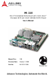
MI-110 Mini-ITX Embedded Motherboard with Intel® Atom™ Processor N270 and Intel® 945GSE/ICH7M Chipset User’s Manual Manual Rev.: 2.00 Revision Date: October 2, 2009 Part No: 50-1Z012-1000 Advance Technologies; Automate the World.
Revision History Revision Release Date 2.
MI-110 Preface Copyright 2009 ADLINK Technology Inc. This document contains proprietary information protected by copyright. All rights are reserved. No part of this manual may be reproduced by any mechanical, electronic, or other means in any form without prior written permission of the manufacturer. Disclaimer The information in this document is subject to change without prior notice in order to improve reliability, design, and function and does not represent a commitment on the part of the manufacturer.
Using this Manual Audience and Scope The MI-110 User’s Manual is intended for hardware technicians and systems operators with knowledge of installing, configuring and operating industrial grade computers. Manual Organization This manual is organized as follows: Preface: Presents copyright notifications, disclaimers, trademarks, and associated information on the proper usage of this document and its associated product(s).
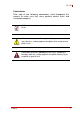
MI-110 Conventions Take note of the following conventions used throughout this manual to make sure that users perform certain tasks and instructions properly. Additional information, aids, and tips that help users perform tasks. NOTE: CAUTION: WARNING: Preface Information to prevent minor physical injury, component damage, data loss, and/or program corruption when trying to complete a task.
This page intentionally left blank.
MI-110 Table of Contents Revision History...................................................................... ii Preface .................................................................................... iii Table of Contents.................................................................. vii List of Figures ........................................................................ ix List of Tables.......................................................................... xi 1 Introduction ............
4.2 Standard CMOS Features ................................................. 35 4.3 Advanced BIOS Features .................................................. 37 4.4 Advanced Chipset Features............................................... 42 4.5 Integrated Peripherals........................................................ 44 4.6 Power Management Setup ................................................ 51 4.7 PnP/PCI Configurations ..................................................... 54 4.
MI-110 List of Figures Figure 1-1: Figure 1-2: Figure 1-3: Figure 1-4: Figure 1-5: MI-110 Block Diagram ..................................................... 5 MI-110 Board Layout ..................................................... 10 MI-110 Rear I/O Layout ................................................. 11 MI-110 Board Dimensions ............................................. 12 Rear I/O Faceplate Dimensions.....................................
This page intentionally left blank.
MI-110 List of Tables Table Table Table Table Table Table Table Table Table Table Table 1-1: 1-2: 1-3: B-1: B-2: B-3: B-4: B-5: B-6: B-7: B-8: List of Tables MI-110 General Specifications......................................... 4 Intel® Atom™ N270 processor Power Consumption ...... 9 MI-110 Board Layout Legend ........................................ 11 System Memory Map..................................................... 65 Direct Memory Access Channels...................................
This page intentionally left blank.
MI-110 1 Introduction This chapter will introduce the MI-110, its features, specifications, functional description, and mechanical layout. 1.1 Package Contents Please check that your package contains the items below. If you discover damaged or missing items, please contact your vendor.
1.2 Overview The ADLINK MI-110 is a Mini-ITX embedded motherboard based on the Intel® Atom™ processor N270 built on 45-nm process technology in Micro-FCBGA8 package and the Mobile Intel® 945GSE + ICH7M Express Chipset. The MI-110 is ideal for embedded applications requiring fanless operation and ultra-low power consumption in a standard small form factor motherboard with a complete set of I/O functions and high-bandwidth network connectivity.
MI-110 1.4 Specifications System CPU Intel® Atom™ processor N270 • 1.6 GHz core frequency • 512KB L2 cache • Micro-FCBGA8 package FSB • 533 MHz Chipset • Mobile Intel® 945GSE + ICH7M Express Chipset Memory • DDR2 533 SDRAM (2GB max.) • 1x 200-pin SO-DIMM slot BIOS • Award BIOS with 16 Mb Flash ROM TPM • TPM 1.2 via Infineon SLB 9635 TT 1.
Display Graphics Processor • Intel® GMA950 integrated in 945GSE supporting dual independent display VRAM • Shared system memory up to 224 MB CRT • Dsub-15 connector up to 2048x1536 @ 75Hz (QXGA) DVI • DVI-I via Chrontel 7307C, up to 1600x1200 (UXGA) LVDS • Dual-channel 18-bit LVDS up to 1600x1200 (UXGA) Controller • Realtek 8111C GbE controller Ports • 2x RJ-45 Ethernet port Ethernet Mechanical and Environment Form Factor • Mini-ITX Embedded Motherboard Dimensions • 170 mm x 170 mm (L x W)
MI-110 1.5 Block Diagram CPU Intel® Atom™ N270 1.6GHz 533 MHz FSB 512K L2 Cache 437-pin Micro-FCBGA8 533 MHz FSB CRT SO-DIMM up to 2GB Northbridge DB-15 Intel® 945GSE GMCH Dual Channel 18-bit LVDS DDRII 533MHz Chrontel 7307C DVI Transmitter DVI DMI Interface 2 GB/s Southbridge PCIe x1 PCIe Mini slot PCIe x1 RTL8111C RJ-45 PCIe x1 RTL8111C RJ-45 PCI Bus PCI 32-bit/ 33MHz bus ® Intel ICH7M IDE / CF SATA ports x2 USB 2.0 (Bracket x4, Internal x2) IDE PCIe Controller SATA USB 2.
1.6 Functional Description Processor Support The MI-110 embedded motherboard is equpped with the Intel® Atom™ N270 processor in Micro-FCBGA8 package. Implemented in 45nm process technology, the Intel® Atom™ N270 is poweroptimized to deliver robust performance per watt for cost-effective embedded applications. Features include: X 1.6 GHz core speed with 533 MHz FSB and 2.
MI-110 Intel® Graphics Media Accelerator GMA 950 The Intel® Graphics Media Accelerator (GMA) 950 provides an integrated 3D graphics engine delivering sophisticated graphics for large display applications. With support for DirectX 9 hardware acceleration, 400 MHz display clock, and up to 224 MB of video memory, the Intel GMA 950 provides a cost-effective and high-performance graphics solution.
Watchdog Timer The watchdog timer (WDT) monitors system operations based on user-defined configurations. The WDT can be programmed for different time-out periods, such as from 1 to 255 seconds or from 1 to 255 minutes. The WDT generates a reset signal, then a reset request, after failure to strobe it within the programmed time period. A register bit may be enabled to indicate if the watchdog timer caused the reset event.
MI-110 1.7 Power Consumption Intel® Atom™ N270 processor, 1.6GHz, 512KB L2 cache, 533MHz FSB Test Configuration Memory Elpida DDR2 667MHz, 2GB Graphics Intel® Graphics Media Accelerator 950 SATA HD WD Caviar SE, WD1600JS-60NCB1, 160GB Power Supply Sunpower SPX-5600P1 500W DOS (idle) Power Req. +5VSB +12V Total Current (mA) – 719.4 – Watts (W) – – 8.633 Windows XP, Idle Power Req. +5V +12V Total Current (mA) – 695.8 – Watts (W) – – 8.
1.
MI-110 AAFP1 Front Panel Audio pin header JCOMPWR1/2 COM1/2 RI, +12V and +5V power select jumper ATXPWR1 ATX Power connector JCOMPWR3/4 COM3/4 RI, +12V and +5V power select jumper CHA_FAN System Fan connector JDIO Digital IO pin header CLRTC Clear CMOS jumper JLVDS1 LVDS connector COM3/4 Serial Port pin headers SATA1/2 SATA1/2 connectors F_PANEL1 System Panel pin header SODIMMA1 SO-DIMM socket IDE1 IDE connector S/PDIF pin header JAMP1 Audio Amplifier connector SPI_JP1 SPI pin he
1.
MI-110 Dimensions in mm Figure 1-5: Rear I/O Faceplate Dimensions Introduction 13
This page intentionally left blank.
MI-110 2 Connectors & Jumpers The connectors and jumpers on the MI-110 allow you to connect and configure external devices. The following specify the pin assignments for connectors and jumper on the MI-110. Refer to Figure 1-2: MI-110 Board Layout and Figure 1-3: MI-110 Rear I/O Layout for connector and jumper locations. 2.
Serial Port Connectors (COM1/2) Pin # RS-232 1 DCD, Data Carrier Detect 2 RXD, Receive Data 3 TXD, Transmit Data 4 DTR, Data Terminal Ready 5 GND, ground 6 DSR, Data Set Ready 7 RTS, Request to Send 8 CTS, Clear to Send 9 RI_Power, Ring Indicator / Power* *Note: See “Jumper Settings” on page 27 for RI/+5V/+12V selection. VGA Connector.
MI-110 DVI-I Connector (CN2) Pin # Signal Pin # Signal 1 TMDS Data2- 16 Hot Plug Detect 2 TMDS Data2+ 17 TMDS Data0- 3 TMDS Data2/4 Shield 18 TMDS Data0+ 4 TMDS Data4- 19 TMDS Data0/5 Shield 5 TMDS Data4+ 20 TMDS Data5- 6 DDC Clock 21 TMDS Data5+ 7 DDC Data 22 TMDS Clock Shield 8 Analog Vertical Sync 23 TMDS Clock + 9 TMDS Data1- 24 TMDS Clock - 10 TMDS Data1+ C1 Analog Red 11 TMDS Data1/3 Shield C2 Analog Green 12 TMDS Data3- C3 Analog Blue 13 TMDS Dat
USB Connectors Pin # Signal Name 1 Vcc 2 USB- 3 USB+ 4 GND LAN Port (RJ-45) This port allows gigabit connection to a Local Area Network (LAN) using a network hub. The LAN port comes with two LEDs to indicate link, activity and speed. Refer to the tables below for the LAN port pin and LED definitions ..
MI-110 2.2 Onboard Connectors Front Panel Audio Pin Header (AAFP1) Pin # Signal Pin # Signal 1 MIC2_L 6 AGND 2 MIC2_R 7 FP_PRES# 3 MIC2_R 8 SRTN1 4 SENSE A 9 Key 5 LIN2_L 10 SRTN2 1 2 ATX Power Connector (ATXPWR1) Pin # Signal Pin # Signal 1 +3.3V 11 +3.3V 2 +3.
Serial Port Connectors (COM3/4) Pin # Signal Functions 1 DCD Data Carrier Detect 2 TXD Transmit Data 3 GND Ground 4 RTS Request to Send 5 RI_Power 6 RXD Receive Data 7 DTR Data Terminal Ready 8 DSR Data Set Ready 9 CTS Clear to Send 10 NC Key 1 6 Ring Indicate, Power * 5 *Note: See “Jumper Settings” on page 27 for RI/+5V/+12V selection.
MI-110 System Panel Connector (F_PANEL1) Pin # Signal 1 HD_LED+ 2 HD_LED- 3 GND 4 RESET 5 NC 6 PWR_LED+ 7 PWR_LED- 8 PWR 9 GND 10 NC Connectors & Jumpers Pin Group Hard Disk LED Reset Button 1 Power LED 5 6 Power Switch 21
IDE Connector (IDE1) Pin # Signal Pin # Signal 1 Reset 2 Ground 3 Data 7 4 Data 8 5 Data 6 6 Data 9 7 Data 5 8 Data 10 9 Data 4 10 Data 11 11 Data 3 12 Data 12 13 Data 2 14 Data 13 15 Data 1 16 Data 14 17 Data 0 18 Data 15 19 Ground 20 - 21 Request 22 Ground 23 I/O Write 24 Ground 25 I/O Read 26 Ground 27 I/O Ready 28 Cable Select 29 DMA Ack 30 Ground 31 Interrupt Request 32 No Connect 33 Device Address 1 34 ATA 66/100 Detect 35 Device
MI-110 LCD Inverter pin header (JBLK1) Pin # Signal 1 +12V 2 GND 3 ENBKL 4 VR 5 +5V 1 Digital IO pin header (JDIO) Pin # Signal Pin # Signal 1 DIO GP20 2 DIO GP10 3 DIO GP21 4 DIO GP11 5 DIO GP22 6 DIO GP12 7 DIO GP23 8 DIO GP13 9 DIO GP24 10 DIO GP14 11 DIO GP25 12 DIO GP15 13 DIO GP26 14 DIO GP16 15 DIO GP27 16 DIO GP17 17 SMBCLK 18 SMBDATA 19 Ground 20 VCC Connectors & Jumpers 1 2 23
LVDS Flat Panel Connector (JLVDS1) 24 Pin # Signal Pin # Signal 2 +5V 1 +3.3V 4 +5V 3 +3.
MI-110 SATA Connectors (SATA1-6) Pin # Signal 1 GND 2 TXP 3 TXN 4 GND 5 RXN 6 RXP 7 GND 1 7 S/PDIF Pin Header (SPDIF_OUT) Pin # Signal 1 +5V 2 NC 3 SPDIF0 4 GND Connectors & Jumpers 1 25
SPI pin header (SPI_JP1) Pin # Signal Pin # Signal 1 +3V ROM 2 GND 3 F_SPI_CS# 4 F_SPI_CLK 5 F_SPI_MISO 6 F_SPI_MOSI 7 SPI_HOLD# 8 NC 1 USB 2.
MI-110 2.3 Jumper Settings Clear CMOS Jumper (CLRTC) The CMOS RAM data contains the date / time and BIOS setting information. CMOS is powered by the onboard button cell battery. To erase the CMOS RAM data: 1. Unplug the MI-110. 2. Short the CLRTC pins 2-3. 3. Remove the jumper cap from pins 2-3 and reinstall it to pins 1-2. Power up the system.
COM1 RI, +12V and +5V Function Select (JCOMPWR1/2) These jumpers allows you to select COM1 RI, +5V and +12V functions. Set JCOMPWR1 to pins 1-3 and JCOMPWR2 to pins 1-3 to select +5V power. Set JCOMPWR1 to pins 3-5 and JCOMPWR2 to pins 1-3 to select +12V power. Set JCOMPWR2 to pins 3-5 and JCOMPWR1 to open for RI selection. COM2 RI, +12V and +5V Function Select (JCOMPWR1/2) These jumpers allow you to select COM2 RI, +5V and +12V power. Set JCOMPWR1 to pins 2-4 and JCOMPWR2 to pins 2-4 to select +5V power.
MI-110 COM3 RI, +12V and +5V Function Select (JCOMPWR3/4) These jumpers allow you to select COM3 RI, +5V and +12V power. Set JCOMPWR3 to pins 1-3 and JCOMPWR4 to pins 1-3 to select +5V power. Set JCOMPWR3 to pins 3-5 and JCOMPWR4 to pins 1-3 to select +12V power. Set JCOMPWR4 to pins 3-5 and JCOMPWR3 to open for RI selection. COM4 RI, +12V and +5V Function Select (JCOMPWR3/4) These jumpers allow you to select COM4 RI, +5V and +12V power.
This page intentionally left blank.
MI-110 3 Getting Started This chapter provides information on how to install components to the MI-110 SBC. 3.1 System Memory The MI-110 supports up to 2 GB of DDR2 400/533 SDRAM in one 200-pin SO-DIMM socket. See Figure 1-2 on page 10 for the SO-DIMM socket location. Memory Module Installation The DDR2 memory modules are notched to facilitate correct installation in the DIMM sockets.
3.2 Driver Installation The MI-110 drivers for Windows XP 32-bit are located in the following directories on the Driver CD, or can be downloaded from the ADLINK website (http://www.adlinktech.com): Chipset X:\MI-110\CHIP\setup.exe Display X:\MI-110\VGA\Win2KXP\win2k_xp14311.exe LAN X:\MI-110\LAN\Win2KXP\setup.exe Audio X:\MI-110\Audio\Windows 32_64\WDM_R182.exe TPM X:\MI-110\TPM\setup.exe Follow the instructions below to install the required MI-110 drivers: 1.
MI-110 4 BIOS Setup The following chapter describes basic navigation for the Phoenix AwardBIOS Setup Utility. 4.1 Starting the BIOS To enter the setup screen, follow these steps: 1. Power on the motherboard 2. Press the key on your keyboard during the Power-On-Self-Test (POST) to enter the Setup utility. 3. After you press the < Delete > key, the main BIOS Setup Menu will be displayed.
Navigation Use the keys described below to navigate through the BIOS Setup Utility Key(s) Function Description F1 General help, only for Status Page Setup Menu and Option Page Setup Menu Esc Return to the main menu from a sub-menu or prompts you to quit the setup program. ←,→ Move to the item on the left or right ↑,↓ Move to previous or next item Enter Brings up a selection menu for the highlighted field.
MI-110 4.2 Standard CMOS Features The main menu includes the following setup categories. Recall that some systems may not include all entries. Date/Time Use this option to change the system time and date. The date must be entered in MM/DD/YY format. The time is entered in HH:MM:SS format. Note: The time is in 24-hour format. For example, 5:30 A.M. appears as 05:30:00, and 5:30 P.M. as 17:30:00. IDE Channel 0/1 Master/Slave This selection brings up the configuration submenu of the designated device.
Capacity: Auto display disk size Disk drive capacity (approximated). Access Mode: CHS/LBA/Large/Auto Selects the access mode for a hard disk The following options are selectable only if the 'IDE Primary Master' item is set to 'Manual' Cylinder: Min = 0 Max = 65535 Sets the number of cylinders for a hard disk.
MI-110 4.3 Advanced BIOS Features This section allows users to configure the Advanced BIOS Features of the system.
CPU Features Delay Prior to Thermal The Delay Prior To Thermal BIOS feature controls the activation of the Thermal Monitor's automatic mode. It allows you to determine when the Pentium 4's Thermal Monitor should be activated in automatic mode after the system boots. For example, with the default value of 16 Minutes, the BIOS activates the Thermal Monitor in automatic mode 16 minutes after the system starts booting up. Limit CPUID MaxVal Set Limit CPUID MaxVa1 to 3.
MI-110 Hard Disk Boot Priority Sets hard disk boot device priority. CH0 S. Primary SATA channel with Master Device. It will show the device model / type when SATA HDD or CD ROM connected. Bootable Add-in Cards "Bootable add-in cards" is an item on the HDD boot priority list. Virus Warning Enables or disables the virus warning. CPU L1 & L2 Cache Enables or disables the CPU L1 & L2 Cache. Enabling this feature speeds up memory access.
Enables or disables the Hyper-Threading function of the CPU. Quick Power On Self Test Speeds up the Power On Self Test (POST). If enabled, the BIOS will shorten the test time or skip some check items during POST. First/Second/Third Boot Device Pressing displays the Boot Device Menu. The BIOS will attempt to load the operating system from the selected devices in sequence. Boot Other Device Enables the BIOS to boot from a second or third device if booting from the first device fails.
MI-110 MPS Version Control for OS This option is only valid for multiprocessor motherboards as it specifies the version of the Multiprocessor Specification (MPS) that the motherboard will use. The MPS is a specification by which PC manufacturers design and build Intel architecture systems with two or more processors. MPS 1.1 was the original specification. MPS version 1.4 adds extended configuration tables for improved support of multiple PCI bus configurations and greater expandability in the future.
4.4 Advanced Chipset Features DRAM Clock/Drive Control When set to “BySPD”, the DRAM timing parameters are set according to DRAM SPD (Serial Presence Detect). When disabled, one can manually set the DRAM timing parameters using the sub items below. Set to “BySPD” if not sure. CAS Latency Time Controls the latency between the SDRAM Read command and the time data actually becomes available. DRAM RAS# to CAS# Delay Controls the latency between the DDR SDRAM active command and the read/write command.
MI-110 System BIOS Cacheable Selecting “Enabled” allows caching of the system BIOS ROM at F0000h- FFFFFh, resulting in better system performance. However, if any pro-gram writes data to this memory area, a system error may occur. Video BIOS Cacheable Selecting Enabled allows caching of the video BIOS ROM at F0000h-FFFFFh, resulting in better video performance. However, if any program writes to this memory area, a system error may result.
4.
MI-110 On Chip IDE Device IDE HDD Block Mode If your IDE hard drive supports block mode select Enabled for automatic detection of the optimal number of block read/writes per sector the drive can support. IDE DMA Transfer Access Use this field to enable or disable IDE DMA transfer access. OnChip Primary/Seondary PCI IDE The integrated peripheral controller contains an IDE interface with support for two IDE channels. Select Enabled to activate each channel separately.
Onboard Device Azalia Audio Select Select [Disabled] if you do not want to use Azalia audio.
MI-110 Super I/O Device Power ON Function This feature allows you to wake up the system using any of the listed options. The selections are “Hot KEY”, “Mouse Left”, “Mouse Right”, “Any KEY” and “BUTTON ONLY” (default). KB Power ON Password The system will ask for a password, after entering the correct password the keyboard can then be used. Hot Key Power ON Awaken the system by pressing the hot key button. The options are “Ctrl-F1”, “Ctrl-F2”, “Ctrl-F3” to “Ctrl-F8”.
This field sets the address of the on-board parallel port connector. You can select “378/IRQ7”, “278/IRQ5”, “3BC/IRQ7”, or “Disabled”. If you install an I/O card with a parallel port, make sure there is no conflict in the address assignments. The single board computer can support up to three parallel ports. PWRON After PWR-Fail Determines which state the computer enters when AC power is restored after a power loss. The options for this value are On, Off, and Former-Sts.
MI-110 USB Device Setting USB Controller The options: Disabled, Enabled. USB 2.0 Controller The options: Disabled, Enabled. USB Operation Mode Allows you to configure the USB 2.0 controller in HiSpeed (480 Mbps) or Full Speed (12 Mbps). Configuration options: [Full/Low Speed] [HiSpeed] USB Keyboard Function The options: Disabled, Enabled. USB Mouse Function The options: Disabled, Enabled. USB Storage Function The options: Disabled, Enabled.
Security Chip Configuration TPM Support The choices are “Enabled” and “Disabled”. TPM Current Status This item shows you the current TPM status. TPM Status The options are “No Change” / “Clear” / “Enable & Activate” / “Deactivate & Disable”.
MI-110 4.6 Power Management Setup ACPI Function The options are “Enabled” and “Disabled”. ACPI Suspend Type This item allows you to set ACPI suspend type to S1/POS (Power On Suspend) or S3/STR (Suspend To RAM). Run VGABIOS if S3 Resume Select “Auto” to run VGA BIOS if S3 resume automatically. The “Yes” enables running VGA BIOS if S3 resume. The “No” disables this function. Power Management There are three selections for Power Management, and each of them has fixed mode settings. X Min.
X Max. Power Saving: Maximum power management, HDD Power Down =1 Min X User Defined: Allows you to set each mode individually. When not disabled, each of the ranges are from 1 min. to 1 hr. except for HDD Power Down which ranges from 1 min. to 15 min. and disable. Video Off Method Use this to select the method to turn off the video. The options are “Blank Screen”, “V/H SYNC+ Blank”, and “DPMS”. Video Off In Suspend When the system is in suspend mode, the video will turn off.
MI-110 Power On by Ring Select “Enabled” to power on the system from a soft off state by an input signal on the serial Ring Indicator (RI) line. The options are “Enabled” and “Disabled”. USB KB Wake-Up from S3 When “Enabled”, enter any key to wake up the system from S3 state. The options are “Enabled” and “Disabled”. Resume by Alarm When “Enabled”, set the date and time at which the RTC (realtime clock) alarm awakens the system from suspend mode. The options are “Enabled” and “Disabled”.
4.7 PnP/PCI Configurations This section describes configuring the PCI (Personal Computer Interconnect) bus system. PCI is a system which allows I/O devices to operate at speeds nearing the speed the CPU itself uses when communicating with its own components. Init Display First This item allows you to choose the first display interface to initiate while booting. The choice is “PCI Slot” or “Onboard”. Reset Configuration Data The default is “Disabled”.
MI-110 PCI/VGA Palette Snoop This is set to “Disabled” by default. INT Pin 1/2/3/4/5/6/7/8 Assignment The options: Auto, 3, 4, 5, 7, 9, 10, 11 Maximum Payload Size This allows you to set the maximum TLP payload size for PCI Express devices. The options are [128 bytes], [256 bytes], [512 bytes], [1024 bytes], [2048 bytes], and [4096 bytes].
4.
MI-110 4.9 Frequency/Voltage Control Auto Detect PCI Clk This allows you to enable or disable auto detect PCI clock. Options: Enabled, Disabled. Spread Spectrum This setting allows you to reduce EMI by modulating the signals the CPU generates so that the spikes are reduced to flatter curves. This is achieved by varying the frequency slightly so that the signal does not use any particular frequency for more than a moment. Options: Enabled, Disabled.
4.10 Load Optimized Defaults Use this menu to load the BIOS default values that are factory settings for optimal performance system operations. Press “Y” to load the default values setting for optimal performance system operations.
MI-110 4.11 Set Supervisor & User Password These two options set the system password. Supervisor Password sets a password that will be used to protect the system and Setup utility. User Password sets a password that will be used exclusively on the system. To specify a password, highlight the type you want and press < Enter >. The “Enter Password:” message prompts you on the screen. Type the password, up to eight characters in length, and press < Enter >.
4.12 Save & Exit Setup This option allows you to determine whether to accept any modifications or not. Typing Y will quit the setup utility and save all changes into the CMOS memory. Typing “N” will return to the Setup Utility Main Screen.
MI-110 4.13 Exit Without Saving Select this option to exit the Setup utility without saving the changes you have made in this session. Typing “Y” will quit the Setup utility without saving any modifications. Typing “N” will return to the Setup utility.
This page intentionally left blank.
MI-110 Appendix A - Watchdog Timer The programming instructions for the MI-110’s Watchdog Timer are as follows. A.
This page intentionally left blank.
MI-110 Appendix B - System Resources B.
B.2 Direct Memory Access Channels Channel Number Data Width System Resource 0 8-bits 1 8-bits Parallel port(1) 2 8-bits Diskette drive(1) 3 8-bits Parallel port(1) 4 8-bits Direct memory access controller 5 16-bits Open 6 16-bits Open 7 16-bits Open Table B-2: Direct Memory Access Channels Note(1): DMA channel 1/3 is selected when using parallel port. Floppy (Winbond default uses DMA 02) and parallel port cannot be used at the same time.
MI-110 B.
B.
MI-110 B.
IRQ Lines APIC Mode IRQ# Typical Interrupt Resource Connected to Pin Note 0 System Timer 3 Communications port (COM2) IRQ3 via SERIRQ, IRQ3 at ISA bus Note (1) 4 Communications port (COM1) IRQ4 via SERIRQ, IRQ4 at ISA bus Note (1) 5 Intel® 82801G (ICH7) SMBus controller - 27DA 8 System CMOS / Real-time clock 9 Microsoft ACPI-compliant system 10 Communications port (COM3) IRQ10 via SERIRQ, IRQ10 at ISA bus Note (1) 11 Communications port (COM4) IRQ11 via SERIRQ, IRQ11 at ISA bus No
MI-110 B.
B.7 PCI Interrupt Routing Map INT Line INT1 Intel VGA compatible Controller X Intel Multimedia device X Intel PCI-to-PCI Bridge X INT2 Intel PCI-to-PCI Bridge INT3 X Intel PCI-to-PCI Bridge Intel UHCI USB Controller X X Intel UHCI USB Controller X Intel UHCI USB Controller X Intel UHCI USB Controller Intel USB v2.
MI-110 Important Safety Instructions For user safety, please read and follow all instructions, WARNINGS, CAUTIONS, and NOTES marked in this manual and on the associated equipment before handling/operating the equipment. X Read these safety instructions carefully. X Keep this user’s manual for future reference. X Read the specifications section of this manual for detailed information on the operating environment of this equipment.
X Never attempt to fix the equipment. Equipment should only be serviced by qualified personnel. A Lithium-type battery may be provided for uninterrupted, backup or emergency power. WARNING: X 74 Risk of explosion if battery is replaced with one of an incorrect type. Dispose of used batteries appropriately.
MI-110 Getting Service Contact us should you require any service or assistance. ADLINK Technology Inc. Address: 9F, No.166 Jian Yi Road, Chungho City, Taipei County 235, Taiwan קᗼխࡉؑ৬ԫሁ 166 ᇆ 9 ᑔ Tel: +886-2-8226-5877 Fax: +886-2-8226-5717 Email: service@adlinktech.com Ampro ADLINK Technology Inc. Address: 5215 Hellyer Avenue, #110, San Jose, CA 95138, USA Tel: +1-408-360-0200 Toll Free: +1-800-966-5200 (USA only) Fax: +1-408-360-0222 Email: info@adlinktech.
ADLINK Technology Inc. (German Liaison Office) Address: Nord Carree 3, 40477 Duesseldorf, Germany Tel: +49-211-495-5552 Fax: +49-211-495-5557 Email: emea@adlinktech.com ADLINK (French Liaison Office) Address: 15 rue Emile Baudot, 91300 MASSY Cedex, France Tel: +33 (0) 1 60 12 35 66 Fax: +33 (0) 1 60 12 35 66 Email: france@adlinktech.com ADLINK Technology Japan Corporation Address: 151-0072 ᧲੩ㇺᷦ⼱ᐈ䊱⼱㩷 1-1-2 ᦺᣣ↢ᐈ䊱⼱䊎䊦 8F Asahiseimei Hatagaya Bldg.