NuIPC / NuDAQ 743X Series 64-CH Isolated Digital I/O Board User’s Guide
Copyright 2002 ADLINK Technology Inc. All Rights Reserved. Manual Rev. 3.34: October 22, 2002 Part NO: 50-11108-202 The information in this document is subject to change without prior notice in order to improve reliability, design and function and does not represent a commitment on the part of the manufacturer.
Getting service from ADLINK • Customer Satisfaction is the most important priority for ADLINK Tech Inc. If you need any help or service, please contact us. ADLINK Technology Inc. Web Site http://www.adlinktech.com Sales & Service Service@adlinktech.com NuDAQ + USBDAQ nudaq@adlinktech.com Automation automation@adlinktech.com NuIPC nuipc@adlinktech.com NuPRO / EBC nupro@adlinktech.com TEL +886-2-82265877 FAX Address 9F, No. 166, Jian Yi Road, Chungho City, Taipei, 235 Taiwan.
Table of Contents Tables and Figures..................................................................iii Introduction ............................................................................... 1 1.1 1.2 1.3 1.4 Features .............................................................................. 2 Applications ......................................................................... 3 Specifications ...................................................................... 3 Supporting Software........
Registers ..................................................................................21 3.1 3.2 3.3 3.4 PCI PnP Registers ............................................................. 21 I/O Address Map ................................................................ 22 Digital Input Register .......................................................... 23 Digital Output Register ....................................................... 24 Operation Theory ...............................................
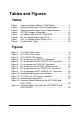
Tables and Figures Tables Table 1. Table 2. Table 3. Table 4. Table 5. Table 6. Table 7. Table 8. Features between different 743X Models ........................ 2 Optical Isolated Input Channel Specifications .................. 3 Optical Isolated Output Channel Specifications ................ 4 PCI-7433 jumper setting table ...................................... 19 I/O Address Map of c/PCI-7432/33/34 ........................... 22 IDI_N: Isolated Digital Input CH N.................................
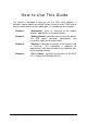
How to Use This Guide This manual is designed to help you use the 743X series products. It describes how to modify and control various functions of the 743X card to meet the requirements of your application. It is divided into four chapters: Chapter 1, “Introduction”, gives an overview of the product features, applications, and specifications. Chapter 2, “Getting Started”, describes how to install the board. The PCB layout, connector specifications, and installation notes are also described.
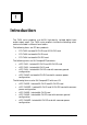
1 Introduction The 743X series products are 64-CH high-density isolated digital input and/or output cards. The 743X series products include the following cards and are available in different form factors.
The above I/O cards are isolated up-to 5000 Vdc (excluding cables) for channel-to-computer isolation. It protects your computer against damage caused by accidental contact with high external voltage and eliminates troublesome ground loops. The 743X series products use PCI-9050 PCI controller to interface the board to the PCI bus. The PCI-9050 fully implements the PCI local bus specification Rev 2.1.
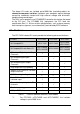
1.2 Applications • • Laboratory and Industrial automation Watchdog timer • Event counter • • Frequency counter and generator Low level pulse generator • Time delay 1.3 Specifications ♦ Optical Isolated Input Channel Number of Channel PCI-7432 cPCI-7432 cPCI-7432R/P PCI-7433 cPCI-7433 cPCI-7433R 32 DI 64 DI Input Voltage 0 – 24V dc logic H: 5~24V logic L: 0~1.5V Input Resistance 2.4KΩ@0.5W (2.
♦ Optical Isolated Output Channel PCI-7432 cPCI-7432 cPCI-7432R/P Number of Channel Output Type PCI-7434 cPCI-7434/P cPCI-7434R/P 32 DO 64 DO Darlington transistor with ground/common power Output Voltage 5VDC min, 35VDC maximum Output Device ULN2803A (common ground) TD62783 (common power) l Sink Current l l common Max. 500mA/ch if only one of the ULN2083A transistor is ON 500mA/ch if all of the ULN2803A transistors are ON @ 20% duty (Tamb = 50? ) Max. 2.
♦ General Specifications Connector: 100-pin SCSI-II connector Operating temperature: 0°C ~ 60°C Storage temperature: -20°C ~ 80°C Humidity: 5 ~ 95%, non-condensing Dimension: • PCI-7432/33/34: Compact size only 106mm(H) X 173mm(L) • • cPCI-7432/33/34: Standard 3U CompactPCI form factor cPCI-7432R/33R/34R: Standard 3U CompactPCI form factor with rear I/O 1.4 Supporting Software ADLINK provides versatile software drivers and packages for users’ different approach to building a system.
• PCIS-DASK: Includes device drivers and DLL for Windows 98, Windows NT and Windows 2000. DLL is binary compatible across Windows 98, Windows NT and Windows 2000. This means a ll applications developed with PCIS-DASK are compatible across Windows 98, Windows NT and Windows 2000. The developing environment can be VB, VC++, Delphi, BC5, or any Windows programming language that allows calls to a DLL. The user’s guide and function reference manual of PCIS-DASK are in the CD.
1.4.5 TM PCIS-DDE: DDE Server and InTouch DDE stands for Dynamic Data Exchange. The PCIS-DDE includes the PCI cards’ DDE server. The PCIS-DDE server is included in the ADLINK CD. It needs a license. The DDE server can be used in conjunction with any DDE client under Windows NT. 1.4.6 PCIS-ISG: ISaGRAF TM driver The ISaGRAF WorkBench is an IEC1131-3 SoftPLC control program development environment. The PCIS-ISG includes ADLINK product drivers for ISaGRAF under Windows NT environment.
2 Getting Started This chapter describes how to install and setup the 743X Series cards. The contents in the package and unpacking information that you should be aware of are outlined first. 2.
2.2 Unpacking The PCI-7432/33/34 card contains electro-static sensitive components that can be easily be damaged by static electricity. Therefore, the card should be handled on a grounded anti-static mat. The operator should be wearing an anti-static wristband, grounded at the same point as the anti-static mat. Inspect the card module carton for obvious damages. Shipping and handling may cause damage to your module. Be sure there are no shipping and handling damages on the modules carton before continuing.
2.3.2 cPCI-743X PCB Layout The CN1 is the I/O interface and is a 100-pin SCSI-type connector. Figure 2: 2.3.3 cPCI-743X PCB Layout cPCI-743XR PCB Layout CN1 is the I/O interface and is a 100-pin SCSI-type connector. J2 is used for rear I/O signaling. There are no connectors on the main board.
2.4 Hardware Installation Outline PCI configuration The PCI cards (or CompactPCI cards) are equipped with plug and play PCI controllers, it can request base addresses and interrupts according to the PCI standard. The system BIOS will assign the system resources based on the PCI cards’ configuration registers and system parameters (which are set by the system BIOS). Interrupt assignment and memory usage (I/O port locations) can only be assigned by the system BIOS.
For cPCI-743X products (with and without rear I/O) 1. Read through this manual, and setup the jumper according to your application needs. 2. Turn off your computer and all accessories (printer, modem, monitor, etc.) connected to the computer. 3. Remove the cover from the slot of your cPCI computer. 4. Select a 32-bit cPCI expansion slot on the back plane for cPCI-743X card. 5.
2.6 Connector Pin Assignment for PCI-7432, cPCI-7432, cPCI-7432R The pin assignment of the 100-pin SCSI-II connector for the 7432 Series is shown in figure 4 below.
2.7 Connector Pin Assignment of cPCI-7432RP The cPCI-7432RP’s pin assignment is shown in Figure 5.
2.8 Connector Pin Assignment of cPCI-7433/R & PCI-7433 The pin assignment of the 100-pin SCSI-II connector for the 7433 Series is shown in figure 6 below.
2.9 Connector Pin Assignment of PCI-7434 The pin assignment of the 100-pin SCSI-II connector for the PCI-7434 Series is shown in figure 7 below.
2.10 Connector Pin Assignment of cPCI-7434R cPCI-7434R’s pin assignment is shown in Figure 8.
2.11 Connector Pin Assignment of cPCI-7434RP cPCI-7434RP’s pin assignment is shown in Figure 9.
2.11 Jumpers Setting Digital I/O cards often operate in noisy environments and may suffer electrostatic discharge or transient voltage up to several 1000 volts. To protect the system from potential damage, the PCI-7433 have implemented protection circuits on its input channels. Eight jumpers on the PCI-7433 are used to enable or disable the transient voltage suppressors. Each jumper is responsible for up to 8 digital input channels. The following table and figure illustrates the jumper settings.
Figure 11: 20 • Getting Started PCI-7433 (rev.
3 Registers The descriptions of the registers and structure of the 743X Series are outlined in this chapter. The information in this chapter will assist programmers, who wish to handle the card with low-level programs. In addition, the low level programming syntax is introduced. This information can help beginners to operate the 743X in the shortest possible time. 3.1 PCI PnP Registers This PCI card functions as a 32-bit PCI target device to any master on the PCI bus.
3.2 I/O Address Map All 743X series registers are 32 bits long. Users can access these registers using 32-bit I/O instructions.
3.3 Digital Input Register There are 32 isolated digital input channels on the PCI-7432 and 64 isolated digital input channels on the PCI-7433, each bit of based address corresponds to a signal on the digital input channel.
3.4 Digital Output Register There are 32 digital output channels on the PCI-7432 and 64 isolated digital output channels on the PCI-7434, each bit of based address corresponds to a signal on the digital output channel.
4 Operation Theory 4.1 Isolated Digital Input Channels The isolated digital input has an open collector transistor structure. The input voltage range is 0V to 24V (0V to 50V for PCI-7433) and the input resistance is 2.4KΩ (4.7KΩ for PCI-7433). The connection between external signals and the 7432/33 is shown in Fig 12. Please note that the input common junction could be common ground or common power, they are dependent on the user’s environment.
4.2 Isolated Digital Output Channels The common ground connection of isolated digital output is shown figure 13, while common power connection of isolated digital output as figure 14. When the isolated digital output goes “ON”, the sink current will be conducted through the transistors. When the isolated digital output goes “OFF”, no current is conducted flow through the transistors.
5 C/C++ Libraries This chapter describes the software libraries for operating this card. Only the functions in the DOS library and Windows 95 DLL are described. Refer to the PCIS-DASK function reference manual, which is included in the ADLINK CD, for descriptions of Windows 98/NT/2000 DLL functions. The function prototypes and useful constants are defined in the header files located in the LIB directory (DOS) and INCLUDE directory (Windows 95).
5.2 Programming Guide 5.2.1 Naming Convention The functions of the NuDAQ PCI or NuIPC CompactPCI card software drivers uses full-names to represent the functions' real meaning. The naming convention rules are: In DOS Environment : _{hardware_model}_{action_name}. e.g. _7432_Initial(). All functions in the PCI-7432 driver have 7432 as {hardware_model} and can be used by both PCI-7432 and cPCI-7432. All functions in the PCI-7433 driver have 7433 as {hardware_model}.
5.3 Running the Testing Utility After installation, execute the DOS utility by typing the following command: C> cd \7432\DOS\UTIL C> 7432UTIL (Use 7433UTIL.EXE or 7434UTIL.EXEdepending on the model of your 743X series card). 5.4 Initial @ Description The 743X cards are initialized by this function. The software library could be used to control multiple 743X cards.
PCI-7434 / cPCI-7434 / cPCI-7434R C/C++ (DOS) U16 _7434_Initial (U16 *existCards, PCI_INFO *pciInfo) C/C++ (Windows 95) U16 W_7434_Initial (U16 *existCards, PCI_INFO *pciInfo) Visual Basic (Windows 95) W_7434_Initial (existCards As Integer, info As PCI_INFO) As Integer @ Argument existCards : The number of installed 7432/33/34 cards. The returned value shows how many 7432/33/34 cards are installed in the system.
5.5 Digital Input Relative Functions @ Description These functions are used to read 32-bit digital inputs data from the digital input port. To obtain a 32-bit data from the 7432, use function “_7432_DI”. To obtain a 32 bit data (MSB double word) from the 7433, use “7433_DI_HiDW”, or use “7433_DI_LoDW” (LSB double word) for the PCI-7433.
5.6 Digital Output Relative Functions @ Description These functions are used to write data to the digital output ports. You can write 32-bit data to the 7432 by using function “_7432_DO”; write 32-bit data (MSB double word) to the 7434 by using “_7434_DO_HiDW”; or write 32-bit data (LSB double word) to 7434 by using “_7434_DO_LoDW”.
5.7 Interrupt Source Control @ Description The 7432 and 7433 both have a dual interrupt system. Two interrupt sources can be generated and be checked by the software. This function is used to select and control the 7432/33 interrupt sources by writing data to the interrupt control register. The interrupt source can be set as Channel 0 (INT1) and/or channel 1 (INT2) of the digital input channels.
5.8 Get Interrupt Status @ Description The 7432 and 7433 both have a dual interrupt system. Two interrupt sources can be generated and be checked by the software. This function is used to distinguish which interrupt is inserted if both INT1 and INT2 are in use.
5.9 Interrupt Enable @ Description This function is only available to Windows 95 drivers. It is used to activate the interrupt controller. After calling this function, every time an interrupt request signal is generated, a software event is signaled. Please refer to the sample program 7432int.c or 7433int.c.
5.10 Interrupt Disable @ Description This function is only available to Windows 95 drivers. This function is used to disable the generation of interrupt signals.
5.11 LED Control Function @ Description The LED control function is only available to the CompactPCI rear I/O version. The cPCI-7432R/33R/34R has four user defined LED’s. This function is used to control the LED’s.
5.12 Get Slot Number @ Description The Get slot number function is only available to the CompactPCI rear I/O version. The slot number is read back from the geographic address, which is defined on the backplane.
Warranty Policy Thank you for choosing ADLINK. To understand your rights and enjoy all the after-sales services we offer, please read the following carefully. 1. Before using ADLINK’s products, please read the user manual and follow the instructions carefully. When sending in damaged products for repair, please attach an RMA application form. 2. All ADLINK products come with a two-year guarantee, free of repair charge.
5. To ensure the speed and quality of product repair, please download an RMA application form from our company website www.adlinktech.com . Damaged products with RMA forms attached receive priority. For further questions, please contact our FAE staff. ADLINK: service@adlinktech.com Test & Measurement Product Segment: NuDAQ@adlinktech.com Automation Product Segment: Automation@adlinktech.com Computer & Communication Product Segment: NuPRO@adlinktech.com; NuIPC@adlinktech.