
User`s guide

Operation Theory • 47
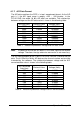
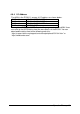
Before performing the D/A conversion, users should take note of the D/A
output range, which is set by JP1. Refer to section 2.4 for jumper setting.
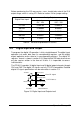
Analog Output
Digital Data Input
Unipolar
0V ~ 10V
Bipolar
-10V ~ 10V
FFF hex +9.9976V +9.9951V
800 hex +5.0000V 0.0000V
7FF hex +4.9976V -0.0049V
000 hex 0.0000V -10.0000V
1 LSB 2.44mV 4.88mV
Table 4: Relationship between DI and AO
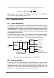
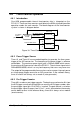
4.5 Digital Input and Output
To program the digital I/O operation is fairly straightforward. The digital input
operation just reads data from its corresponding registers, and the digital
output operation writes data to its corresponding registers. The digital I/O
registers ‘ format is shown in section 3.15. Note that the DIO data channel can
only be read or written in the form of 16 bits. It is impossible to access
individual bits.
The PCI-9111 provides 16 digital input and 16 digital output channels through
CN1 and CN2. The digital I/O signals are fully TTL/DTL compatible. Detailed
digital I/O signal specification can be referred to in section 1.3.
Digital Output (DO)
Digital GND (DGND)
Digital Input(DI)
From TTL Signal
To TTL Devices
PCI-9111
Outside Device
74LS244
74LS373
Figure 15. Digital Input and Output circuit