NuPRO-841 Full-Size Single Board Computer User’s Guide Rev. 1.
© Copyright 2003 ADLINK Technology Inc. All Rights Reserved. Manual Rev. 1.10: September 22, 2003 Part Number: The information in this document is subject to change without prior notice in order to improve reliability, design and function and does not represent a commitment on the part of the manufacturer.
Getting service from ADLINK • Customer Satisfaction is the most important priority for ADLINK Tech Inc. If you need any help or service, please contact us. ADLINK Technology Inc. Web Site http://www.adlinktech.com Sales & Service Service@adlinktech.com NuDAQ + USBDAQ nudaq@adlinktech.com Technical Automation automation@adlinktech.com Support NuIPC nuipc@adlinktech.com TEL +886-2-82265877 NuPRO / EBC Address • nupro@adlinktech.com FAX +886-2-82265717 9F, No.
CONTENTS SECTION 1 INTRODUCTION 1.1 Unpacking NuPRO-841 Series 1.2 Description 1.3 Features 1.3.1 Hardware Monitoring 1.3.2 I/O Shield Connector 1.3.3 NuPRO-841 Series Overview 1.3.4 System Block Diagram 1.4 Specifications 1 1 3 3 4 4 4 5 6 SECTION 2 INSTALLATIONS 2.1 System Installation 2.1.1 CPU Installation 2.1.2 Heat Sink Installation 2.1.3 Memory Module Installation 2.1.4 Setting Jumper and DIP Switches 2.2 Board Layout 2.3 Jumper Setting 2.4 Connector’s Description 2.
CONTENTS SECTION 3 AWARD BIOS SETUP 3.1 BIOS Instructions 3.2 Main Menu 3.3 Standard CMOS Features 3.4 IDE Adapters 3.5 Advanced BIOS Features 3.6 Advanced Chipset Features 3.7 Integrated Peripherals 3.8 Power Management Setup 3.9 PnP/PCI Configurations 3.10 PC Health Status 3.11 Frequency/Voltage Control 3.12 Load Fail-Safe Default 3.13 Load Optimized Defaults 3.14 Supervisor/User Password Setting 3.
iv
SECTION 1 INTRODUCTION 1.1 Unpacking NuPRO-841 Series 1. Take out the NuPRO-841 series unit from the carton box, check if the unit is properly secure in the plastic bag. 2.
Introduction ¡ K/B & M/S Y type cable ¡ Driver CD ¡ K/B-M/S extend to BP cable (6-pins to 5-pins) ¡ ATX power control cable (4-pins to 5-pins) ¡ USB 2.0 cable (1 Set) 3.
Introduction 1.2 Description The NuPRO-841 Series single board computer is optimized for socket 478 FC-PGA processor, supporting 533/400MHz Front Side Bus, the memory can accommodate is up to 2GB DDR266/333 SDRAM. This board is based on the Intel® 845GV chipset and is fully designed for harsh industrial environment. The NuPRO-841 series is 533MHz FSB with chipset (GMCH) on-die VGA and one 10/100 Mbps Ethernet controllers. It is for CTI and high-performance applications.
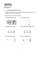
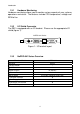
Introduction 1.3.1 Hardware Monitoring Hardware monitoring allows you to monitor various aspects of your systems operations and status. The features include CPU temperature, voltage and RPM of fan. 1.3.2 I/O Shield Connector The SBC is equipped with an I/O bracket. Please use the appropriate I/O shield (figure 1). NuPRO-841 Series KB MS Figure 1: I/O bracket layout 1.3.
Introduction 1.3.
Introduction 1.4 Specifications NuPRO-841: ¡ Processor: - Socket 478 Processors, for Intel® Pentium® 4/ Celeron® Processor ¡ Chipset: - Intel® 845GV AGPset ¡ Front Side Bus: - 400 / 533 MHz ¡ DRAM Module: - 184pins DIMM x 2 for DDR SDRAM up to 2GB (max.
Introduction ¡ USB 2.0 Ports: - 4 x USB 2.0 ports (pin-header) ¡ BIOS: - Award Plug & Play BIOS ¡ Extended Function: - Hardware Monitoring function - IrDA by pin-header ¡ Form Factor: - 13.3” x 4.8” (338 x 122mm) ¡ Weight: - 0.
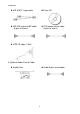
SECTION 2 INSTALLATIONS 2.1 System Installation 2.1.1 CPU Installation Carefully follow the steps below in order to install the CPU: 1. Check and confirm that the jumpers are correctly set for the CPU you are going to install (figure 3). 2. Lift the releasing lever of the Socket 478. 3. Align the pins of the CPU against the pinholes of the Socket 478. Be sure to pay attention to the orientation of the CPU. Figure 3: CPU Socket 4. Push down the CPU into the Socket 478. 5.
Installations Removing a CPU: 1. Before removing the CPU, turn off the NuPRO-841 Series power; then wait for about 3 minutes until the heat radiation plate of the cooling fan and the CPU cool down. 2. To remove the CPU, lift the releasing lever of the Socket 478. Note: The CPU and the heat radiation plate are hot. They may cause burns. To remove the CPU, reverse the installation steps. 2.1.
Installations 2.1.3 Memory Module Installation Figure 5 display the notch marks and what they should look like on your DIMM memory module. DIMMs have184-pins and two notches, that will match with the onboard DIMM socket. DIMM modules are installed by placing the chip firmly into the socket at a 90-degree angle and pressing straight down (figure 6) until it fits tightly into the DIMM socket.
Installations 5. If DIMM does not go in smoothly, do not force it. Pull it all the way out and try again. 6. Make sure the DIMM is properly installed and locked by the tabs on both sides of the socket. Removing a DIMM: To remove the DIMM, use your fingers or a small screwdriver to carefully push away the plastic tabs that secure the DIMM at each end. Lift it out of the socket. Make sure you store the DIMM in an anti-static bag and must be populated the same size and manufactory of memory modules. . 2.1.
Installations 2.2 Board Layout Jumper & Connector Location CN13 CN16 CN19 CN18 JP1 CN5 CN12 CN14 CN11 JP3 CN2 CN4 CN9 CN10 DIMM1 DIMM2 JP2 BATT1 CN21 CN1 CN8 CN7 BZ1 CN6 CN3 NuPRO-841 REV1.
Installations 2.3 Jumper Setting Table for Jumper Location Description: Use the information in the following table to change the jumpers and the DIP switches.
Installations In order to set up the correct configuration, here is the description about how to set the jumpers to enable/disable or change functions. All jumpers’ location please refer to jumper location diagram. COM Port Setting Select: JP1 Function RS-232 (Default) RS-422 RS-485 JP1 1-2 Off On (Term.) On On (Term.) On 3-4 Off (Term.) (Term.
Installations Clear CMOS Setting Select: JP3 Function JP3 Normal (Default) Clear CMOS 1-2 2-3 y Location: 15
Installations 2.4 Connector’s Description Connector Location CN13 CN16 CN19 CN18 JP1 CN5 CN12 CN14 CN11 JP3 CN2 CN4 CN9 CN10 DIMM1 DIMM2 JP2 BATT1 CN21 CN1 CN8 CN7 BZ1 CN6 CN3 NuPRO-841 REV1.
Installations Table for Connector’s Location Description: Use the information in the following table to change the connector.
Installations System Panel Indicate Connector: CN1 Pin # Assignment Pin # IR 1 3 5 7 9 +5V FIRTX IRRX Ground IRTX 2 4 HDLED+ HDLED- SPKR (Default) BUZZ (Default) Ground +5V PWR LED PWR ON 23 25 RESET+ RESET- SPEAKER 8 10 12 14 HDD LED 13 15 Assignment RESET 18 20 22 PWRBT+ PWRBT- PWLED+ NC PWLED- KEYLOCK 24 26 KBLOCK Ground y Figure: 18 2 26 1 25
Installations Primary IDE Connector (40-pins 2.
Installations ATX 12V Power Connector: CN3 Pin # Assignment 1 3 Ground +12V Pin # Assignment 2 4 Ground +12V y Figure: 20 4 3 2 1
Installations Secondary IDE Connector (40-pins 2.
Installations COM2 RS-232/422/485 Serial Port Connector (14-pins 2.
Installations ATX Control Power Connector: CN6 Pin # 1 2 3 4 Assignment PME 5VSB PWRON Ground y Figure: 1 4 FAN2 System(Chassis) Power Connector: CN7 Pin # Assignment 1 2 3 Ground +12V Fan Status Signal y Figure: 1 FAN1 CPU Power Connector: CN8 Pin # 1 2 3 3 Assignment Ground +12V Fan Status Signal y Figure: 1 23 3
Installations Floppy Disk Connector (34-pins 2.
Installations Parallel Port Connector (26-pins 2.
Installations USB2/3 Port Connector (9-pins Pin-Header): CN12 Pin # Assignment Pin # Assignment 1 3 5 7 9 VCC USB2 N USB2 P Ground --- 2 4 6 8 10 VCC USB3 N USB3 P Ground NC y Figure: 1 2 9 10 COM1 RS-232 Serial Port Connector (D-Sub 9-pins Male): CN13 Pin # Assignment Pin # Assignment 1 2 3 4 5 DCD (Data Carrier Detect) RXD (Receive Data) TXD (Transmit Data) DTR (Data Terminal Ready) Ground 6 7 8 9 DSR (Data Set Ready) RTS (Request to Send) CTS (Clear to Send) RI (Ring Indicator) y Figure:
Installations LAN (82562ET) RJ-45 Connector (RJ-45 Phone-jacket): CN14 Pin # Assignment Pin # Assignment 1 2 3 4 Transmit output (+) Transmit output (-) Receive input (+) NC 5 6 7 8 NC Receive input (-) NC NC y Figure: CRT VGA Port Connector (D-SUB 15-pins Female): CN16 Pin # Assignment Pin # Assignment 1 3 5 7 9 11 13 15 Red Color Signal Blue Color Signal Ground Ground 5V 5V H-Sync. SPCLK 2 4 6 8 10 12 14 Green Color Signal 5V Ground Ground Ground VGA DDA V-Sync.
Installations External Keyboard & Mouse Connector (6-pins): CN18 Pin # Assignment Pin # Assignment 1 3 5 Mouse Clock Keyboard Clock Ground 2 4 6 Mouse Data Keyboard Data +5V y Figure: 1 6 PS/2 Keyboard/Mouse Connector (Mini Din 6 Pins): CN19 Pin # Assignment Pin # Assignment 1 3 5 Keyboard Data Ground Keyboard Clock 2 4 6 Mouse Data +5V Mouse Clock y Figure: 6 5 4 3 2 28 1
Installations Extension Audio Connector (9-pins Pin-Header): CN21 Pin # Assignment 1 2 3 4 5 6 7 8 9 +12V 3.
Installations 2.5 Optional Audio Card Board Location: Thank you for select Audio Card, here is the description about how to connect the connector and phone jack to use audio functions. CN2 CN1 CD_IN 1.
Installations 2.
Installations 3. Description of Connector: CD_IN Connector: JP1 Pin # Assignment 1 2 3 4 Left Ground Ground Right Audio Line_In, Line_Out, MIC Phone Jack: CN1 Pin # Assignment 1 2 3 Line_In Line_Out MIC Audio Signal Connector (9-pins): CN2 Pin # 1 2 3 4 5 6 7 8 9 Assignment +12V 3.
SECTION 3 AWARD BIOS SETUP 3.1 BIOS Instructions Award’s ROM BIOS provides a built-in Setup program, which allows user to modify the basic system configuration and hardware parameters. The modified data will be stored in a battery-backed CMOS, so that data will be retained even when the power is turned off. In general, the information saved in the CMOS RAM will stay unchanged unless there is a configuration change in the system, such as hard drive replacement or a device is added.
Award BIOS Setup 3.2 Main Menu Once you enter the AwardBIOS™ CMOS Setup Utility, the Main Menu will appear on the screen. The Main Menu allows you to select from several setup functions and two exit choices. Use the arrow keys to select among the items and press to accept and enter the sub-menu.
Award BIOS Setup Integrated Peripherals: Use this menu to specify your settings for integrated peripherals. See section 4 for the details. Power Management Setup: Use this menu to specify your settings for power management. See section 5 for the details. PnP / PCI Configuration: This entry appears if your system supports PnP / PCI. See section 6 for the details. PC Health Status: Use this menu to show your system temperature, speed and voltage status.
Award BIOS Setup 3.3 Standard CMOS Features The items in Standard CMOS Setup Menu are divided into 10 categories. Each category includes no, one or more than one setup items. Use the arrow keys to highlight the item and then use the or keys to select the value you want in each item.
Award BIOS Setup IDE Secondary Master: Options are in its sub menu (described in 3.4) Press to enter the sub menu of detailed options. IDE Secondary Master: Options are in its sub menu (described in 3.4) Press to enter the sub menu of detailed options. Drive A/ Drive B: Options None 360K, 5.25 in/1.2M, 5.25 in/720K, 3.5 in/ 1.44M, 3.5 in/2.88M, 3.5 in Select the type of floppy disk drive installed in your system. Video: Options EGA/VGA/CGA 40/CGA 80/MONO Select the default video device.
Award BIOS Setup 3.4 IDE Adapters The IDE adapters control the hard disk drive. Use a separate sub menu to configure each hard disk drive. Phoenix - AwardBIOS CMOS Setup Utility IDE Primary Master IDE HDD Auto-Detection Press Enter Item Help ____________________________ IDE Primary Master Access Mode Auto Auto Menu Level Capacity 13579 MB Cylinder Head Precomp Landing Zone Sector 26310 16 0 26309 63 ¾¾ To auto-detect the HDD’s size, head...
Award BIOS Setup The following options are selectable only if the ‘IDE Primary Master’ item is set to ‘Manual’ Cylinder: Options Min = 0, Max = 65535 Set the number of cylinders for this hard disk.
Award BIOS Setup 3.5 Advanced BIOS Features This section allows you to configure your system for basic operation. You have the opportunity to select the system’s default speed, boot-up sequence, keyboard operation, shadowing and security.
Award BIOS Setup CPU L1& L2 Cache: These two categories speed up memory access. However, it depends on CPU/chipset design. Enabled---Enable cache Disabled---Disable cache CPU Hyper-Threading: Allow you to choose the CPU Hyper-Threading Technology. Enabled---Enable CPU Hyper-Threading Disabled--- Disabled CPU Hyper-Threading Quick Power On Self Test: This category speeds up Power On Self Test (POST) after you power up the computer.
Award BIOS Setup Boot Up NumLock Status: Select power on state for NumLock. The choice: On, Off Gate A20 Option: Select if chipset or keyboard controller should control GateA20. Normal---A pin in the keyboard controller controls GateA20 Fast---Lets chipset control GateA20 Typematic Rate Setting: Keystrokes repeat at a rate determined by the keyboard controller. When enabled, the typematic rate and typematic delay can be selected. The choice: Enabled, Disabled.
Award BIOS Setup APIC Mode: This item allows you to enable/disable APIC Mode. The choice: Enabled, Disabled. MPS Version Control For OS: Select the operating system that is Multi-Processors Version Control for OS. The choice: 1.4, 1.1. OS Select For DRAM > 64MB: Select the operating system that is running with greater than 64MB of RAM on the system. The choice: Non-OS2, OS2. Report No FDD For Win 95: Whether report no FDD for Win 95 or not. The choice: Yes, No.
Award BIOS Setup 3.6 Advanced Chipset Features This section allows you to configure the system based on the specific features of the installed chipset. This chipset manages bus speeds and access to system memory resources, such as DRAM and the external cache. It also coordinates communications between the conventional ISA bus and the PCI bus. It must be stated that these items should never need to be altered.
Award BIOS Setup CAS Latency Time: When synchronous DRAM is installed, the number of clock cycles of CAS latency depends on the DRAM timing. The choice: 1.5, 2, and 2.5. Active To Precharge Delay: Select the operating system that is active to precharge delay. The choice: 5, 6, 7 DRAM RAS# to CAS# Delay: You can select RAS to CAS Delay time in HCLKs of 2/2 or 3/3. The system board designer should set the values in this field, depending on the DRAM installed.
Award BIOS Setup Video BIOS Cacheable: Select “Enabled” allows caching of the video BIOS, resulting in better system performance. However, if any program writes to this memory area, a system error may result. The choice: Enabled, Disabled. Memory Hole At 15M-16M: You can reserve this area of system memory for ISA adapter ROM. When this area is reserved, it cannot be cached. The user information of peripherals that need to use this area of system memory usually discusses their memory requirements.
Award BIOS Setup 3.7 Integrated Peripherals Phoenix - AwardBIOS CMOS Setup Utility Integrated Peripherals On-Chip Primary PCI IDE IDE Primary Master PIO IDE Primary Slave PIO IDE Primary Master UDMA IDE Primary Slave UDMA On-Chip Secondary PCI IDE IDE Secondary Master PIO IDE Secondary Slave PIO IDE Secondary Master UDMA IDE Secondary Slave UDMA USB Controller USB 2.
Award BIOS Setup IDE Primary/Secondary Master/Slave PIO: The four IDE PIO (Programmed Input/Output) fields let you set a PIO mode (0-4) for each of the four IDE devices that the onboard IDE interface supports. Modes 0 through 4 provide successively increased performance. In Auto mode, the system automatically determines the best mode for each device. The choice: Auto, Mode 0, Mode 1, Mode 2, Mode 3 and Mode 4.
Award BIOS Setup Init Display First: This item allows you to decide to active whether PCI Slot or on-chip VGA first. The choice: PCI Slot, Onboard. IDE HDD Block Mode: Block mode is also called block transfer, multiple commands, or multiple sector read/write. If your IDE hard drive supports block mode (most new drives do), select Enabled for automatic detection of the optimal number of block read/writes per sector the drive can support.
Award BIOS Setup IR Transmission Delay: This item allows you to enable/disable IR transmission delay. The choice: Enabled, Disabled. UR2 Duplex Mode: This item allows you to select the IR half/full duplex function. The choice: Half, Full. Use IR Pins: This item allows you to select IR transmission routes, one is RxD2m, TxD2 (COM Port) and the other is IR-Rx2Tx2. The choice: IR-Rx2Tx2, RxD2 and TxD2.
Award BIOS Setup 3.8 Power Management Setup The Power Management Setup allows you to configure you system to most effectively save energy while operating in a manner consistent with your own style of computer use.
Award BIOS Setup Power Management: This category allows you to select the type (or degree) of power saving and is directly related to the following modes: 1. HDD Power Down 2. Doze Mode 3. Suspend Mode Min. Power Saving: Minimum power management. Doze Mode = 1 hr. Standby Mode = 1 hr., Suspend Mode = 1 hr., and HDD Power Down = 15 min. Max. Power Saving: Maximum power management -- ONLY AVAILABLE FOR SL CPU’s. Doze Mode = 1 min., Standby Mode = 1 min., Suspend Mode = 1 min., and HDD Power Down = 1 min.
Award BIOS Setup Video Off In Suspend: This determines the manner in which the monitor is blanked. The choice: Yes, No. Suspend Type: Select the Suspend Type. The choice: PwrOn Suspend, Stop Grant. MODEM Use IRQ: This determines the IRQ in which the MODEM can use. The choice: 3, 4, 5, 7, 9, 10, 11 and NA. Suspend Mode: When “Enabled” and after the set time of system inactivity. All devices except the CPU will be shut off. The choice: Disabled, 1, 2, 4, 8, 12, 20, 30, 40 Min and 1Hour.
Award BIOS Setup Power On by Ring: An input signal on the serial Ring Indicator (RI) line (in other words, an incoming call on the modem) awakens the system from a soft off state. The choice: Enabled, Disabled. Resume by Alarm: When “Enabled”, your can set the date and time at which the RTC (real-time clock) alarm awakens the system from Suspend mode. The choice: Enabled, Disabled.
Award BIOS Setup 3.9 PnP/PCI Configurations This section describes configuring the PCI bus system. PCI, or Personal Computer Interconnect, is a system, which allows I/O devices to operate at speeds nearing the speed the CPU itself uses when communicating with its own special components. This section covers some very technical items and it is strongly recommended that only experienced users should make any changes to the default settings.
Award BIOS Setup Resource controlled by: The Award Plug and Play BIOS has the capacity to automatically configure all of the boot and Plug and Play compatible devices. However, this capability means absolutely nothing unless you are using a Plug and Play operating system such as Windows®95. If you set this field to “Manual” choose specific resources by going into each of the sub menu that follows this field (a sub menu is preceded by a “¾”). The choice: Auto (ESCD), Manual.
Award BIOS Setup 3.10 PC Health Status Phoenix - AwardBIOS CMOS Setup Utility PC Health Status CPU Warning Temperature Current System Temp. Current CPU1 Temperature Current CPU Fan Speed Current Chassis Fan Speed VDimm (V) Vcore (V) VCC3.3V +5V +12 V -12 V -5V VBAT (V) 5VSB (V) Shutdown temperature Disabled 33°C / 91°F 38°C / 100°F 3835 RPM 4725RPM 2.48V 1.45V 3.37V 5.08V 11.91V -12.44 -4.99V 3.24V 4.
Award BIOS Setup Vcore (V) Show you the voltage level of CPU (Vcore). VCC3.3V/+5V/+12V/-12V/-5V/5VSB(V): Show you the voltage of 3.3V/+5V/+12V/-12V/-5V. VBAT (V) Show you the voltage level of the battery. Shutdown Temperature: This item allows you to set up the CPU shutdown Temperature. This item is only effective under Windows® 98 ACPI mode. The choice: Disabled, 60°C / 140°F, 65°C / 149°F, 70°C / 158°F and 75°C / 167°F.
Award BIOS Setup 3.11 Frequency/Voltage Control Phoenix - AwardBIOS CMOS Setup Utility Frequency/Voltage Control CPU Clock Ratio Auto Detect PCI Clk Spread Spectrum Item Help ____________________________ 19X Enabled Disabled Menu Level ¾ ↑↓←→Move Enter: Select +/-/PU/PD: Value F10: Save ESC: Exit F1: General Help F5: Previous Values F6: Fail-safe defaults F7: Optimized Defaults CPU Clock Ratio: Use this item to select a multiplier for the system front side bus frequency.
Award BIOS Setup 3.12 Load Fail-Safe Defaults When you press on this item you get a confirmation dialog box with a message similar to: Load Fail-Safe Defaults (Y/N)? N Pressing “Y” loads the BIOS default values for the most stable, minimal-performance system operations.
Award BIOS Setup 3.13 Load Optimized Defaults When you press on this item you get a confirmation dialog box with a message similar to: Load Optimized Defaults (Y/N)? N Pressing “Y” loads the default values that are factory settings for optimal performance system operations.
Award BIOS Setup 3.14 Supervisor/User Password Setting You can set either supervisor or user password, or both of then. The differences between are: Set Supervisor Password: can enter and change the options of the setup menus. Set User Password: just can only enter but do not have the right to change the options of the setup menus. When you select this function, the following message will appear at the center of the screen to assist you in creating a password.
Award BIOS Setup 3.15 Exit Selecting Save & Exit Setup Pressing on this item asks for confirmation: Save to CMOS and EXIT (Y/N)? Y Pressing “Y” stores the selections made in the menus in CMOS – a special section of memory that stays on after you turn your system off. The next time you boot your computer, the BIOS configures your system according to the Setup selections stored in CMOS. After saving the values the system is restarted again.
Warranty Policy Warranty Policy Thank you for choosing ADLINK. To understand your rights and enjoy all the after-sales services we offer, please read the following carefully. 1. Before using ADLINK’s products, please read the user manual and follow the instructions exactly. When sending in damaged products for repair, please attach an RMA application form. 2. All ADLINK products come with a two-year guarantee, free of repair charge.
Warranty Policy 4. Customers are responsible for the fees regarding transportation of damaged products to our company or to the sales office. 5. To ensure the speed and quality of product repair, please download an RMA application form from our company website www.adlinktech.com. Damaged products with RMA forms attached receive priority. For further questions, please contact our FAE staff. ADLINK: service@adlinktech.com Test & Measurement Product Segment: NuDAQ@adlinktech.