Express-BASE User’s Manual Manual Revision: 2.
Revision History Page 2 Release Date Change 2.00 2.10 2.20 2006/9/15 2007/10/19 2009/03/05 2.21 2010/06/11 2.
Table of Contents Preface ............................................................................................................................ 5 1 Introduction ............................................................................................................... 7 2 Special Features ....................................................................................................... 8 2.1 2.2 2.3 2.4 2.5 Primary LPC based Super I/O.........................................................
6.19 6.17 6.20 Power Jumper Settings ....................................................................................................... 32 Other Connectors ................................................................................................................ 33 Other Jumper Settings ........................................................................................................ 35 7 Secondary BIOS.......................................................................................
Preface Copyright 2006-2011 ADLINK Technology, Inc. This document contains proprietary information protected by copyright. All rights are reserved. No part of this manual may be reproduced by any mechanical, electronic, or other means in any form without prior written permission of the manufacturer. Disclaimer The information in this document is subject to change without prior notice in order to improve reliability, design, and function and does not represent a commitment on the part of the manufacturer.
Conventions Take note of the following conventions used throughout this manual to make sure that users perform certain tasks and instructions properly. Additional information, aids, and tips that help users perform tasks. Information to prevent minor physical injury, component damage, data loss, and/or program corruption when trying to complete a task. Information to prevent serious physical injury, component damage, data loss, and/or program corruption when trying to complete a specific task.
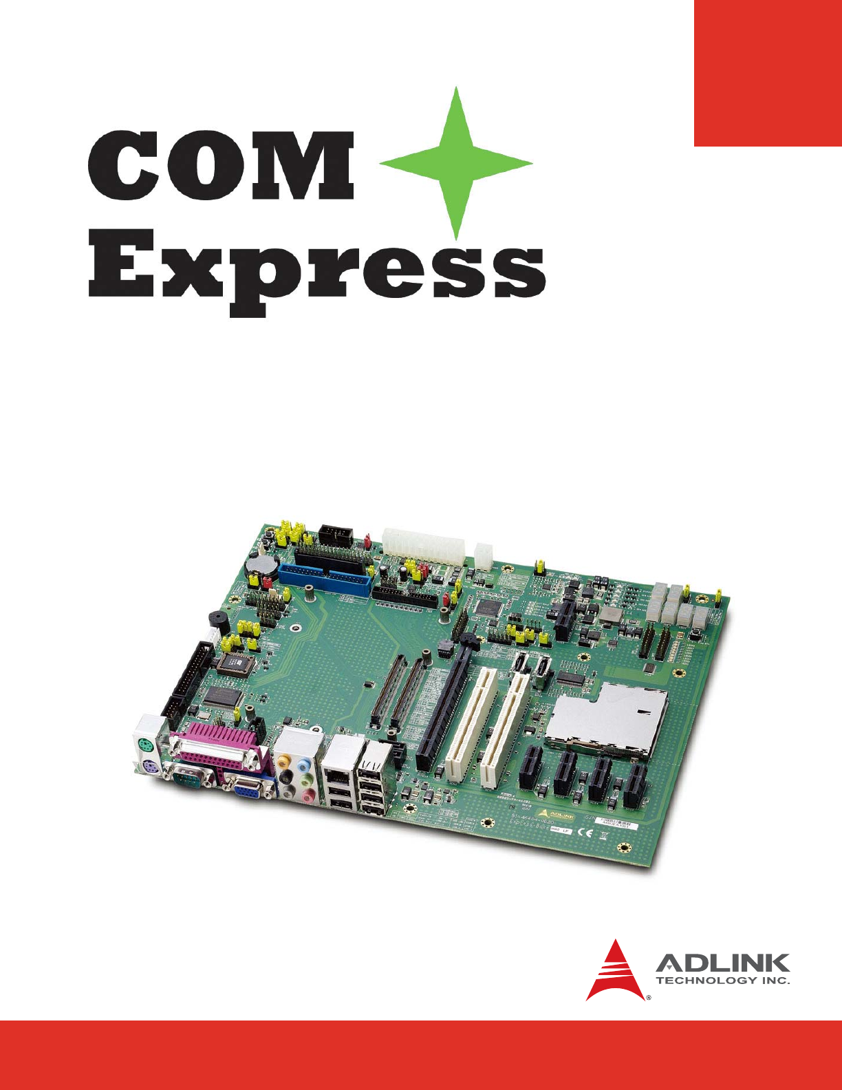
1 Introduction The COM Express approach of custom carrier combined with off the shelf system cores is an excellent solution when you need to customize but lack the time or quantity for a complete redesign. It fits most system integration projects with production volumes from 500 to 10,000 pcs per year.
2 Special Features 2.1 Primary LPC based Super I/O COM Express modules do not have a Super I/O chip onboard as this is considered legacy. Therefore, a Super I/O is placed on the carrier board as an optional item. The Express-BASE uses a Winbond W83627HG-AW that supports FDD, LPT, COM and PS/2 Keyboard and Mouse. 2.2 Secondary BIOS The Express-BASE using firmware hub (FWH) for COM.0 Rev. 1.0 modules and Serial Peripheral Interface (SPI) for COM.0 Rev. 2.0 modules.
SW2 PCIE5 LEDX8 – X1 CNY2 PCIE4 CNY3 51-46604-0D20 Express-BASE 8 8 8 8 8 8 LED13 LED14 JPA2 LED9 JP1 LED10 LED11 LED12 3 Component Location LED15 LED16 LED17 LED18 LED19 PCIE2 PCIE1 PCIE6 LED21 PCIE3 LED2 LED20 PCI2 JPY4 CN30 CNY6 CN11 JPY5 JPY2 CN12 PCIA1 CN40 JPY3 CN31 CNY1 PCIE7 UZ3 JP3 CN6 CN21 JP4 JPZ3 CN13 JP8 JP7 JPY9 CN20 CN7 CNZ1 CN16 CNY8 CN2 JPZ4 CN1 ALC 883 CNY4 JPY11 CNY5 JPZ2 JPZ1 CN41 CN9 CN42 CN17 CN32 JPY10 CN15 CNY9 CN35 CNY7 JPA1 U
4 Function Block Diagram LPT1 COM1 W83627HG COM2 Primary Super I/O KB/MS FDD Debug Header LPC PCI Express x16 onboard slot Secondary BIOS PCI Express Graphics x16 POST Code Display 4 onboard SATA headers Onboard IDE Connector AB CD SATA ALC888 Codec Audio on Rear I/O Gigabit Ethernet Rear I/O PATA CRT VGA Rear I/O LVDS headers PCI Express PCI 2 32-bit PCI Express Card USB Page 10 PP CCPP P I I CC C I EE I I E 11 E 1E 15 6x USB on Rear I/O 1x USB on header Express-BASE User’s Manual
5 Mechanical Dimensions All tolerances ± 0.05 mm Other tolerances ± 0.
6 Connectors and Pin-outs 6.1 Carrier Board Signals AB Connector CD Connector 1 Gigabit Ethernet port Parallel ATA, IDE port alternate definition assigns this to 2 additional Gigabit Ethernet ports LPC interface 4 Serial ATA channels 32-bit PCI v2.3 bus High Definition Audio alternate definition assigns this to 10 additional PCI Express x1 lanes 8 USB 2.
6.4 COM Express Board-to-Board Connectors Signals and Pinout for: Basic form factor, Type 2. Row A Pin No.
COM Express Board-to-Board Connectors (cont'd): Row A Pin No.
6.5 PCI Express and PCI Express Graphic (PEG) Slots PCI Express x1: PCIE1 PCIE2 PCIE4 PCIE5 PCIE6 CN44: B1 A1 B11 B12 A11 A12 B18 A18 ExpressCard (PCIE3, USB7) Express-BASE User’s Manual Pin Signal Pin Signal B1 B2 B3 B4 B5 B6 B7 B8 B9 B10 B11 B12 B13 B14 B15 B16 B17 B18 + 12V + 12V NC GND SMB_CK SMB_DAT GND + 3.3V TRST# +3.3VSB WAKE# NC GND PETp0 PETn0 GND NC GND A1 A2 A3 A4 A5 A6 A7 A8 A9 A10 A11 A12 A13 A14 A15 A16 A17 A18 NC + 12V + 12V GND TCK TDI NC TMS + 3.3V + 3.
PCIE7: PCI Express x16 mode See the JP6 jumper description for PCI Express x16 mode and SDVO mode settings on p. 35. Pin Signal Pin Signal B1 B2 B3 B4 B5 B6 B7 B8 B9 B10 B11 B12 B13 B14 B15 B16 B17 B18 B19 B20 B21 B22 B23 B24 B25 B26 B27 B28 B29 B30 B31 B32 B33 B34 B35 B36 B37 B38 B39 B40 B41 + 12V + 12V NC GND SMB_CK SMB_DAT GND + 3.3V TRST# +3.
PCIE7: SDVO mode See the JP6 jumper description for PCI Express x16 mode and SDVO mode settings on p. 35. Pin Signal Pin Signal B1 B2 B3 B4 B5 B6 B7 B8 B9 B10 B11 B12 B13 B14 B15 B16 B17 B18 B19 B20 B21 B22 B23 B24 B25 B26 B27 B28 B29 B30 B31 B32 B33 B34 B35 B36 B37 B38 B39 B40 B41 + 12V + 12V NC GND SMB_CK SMB_DAT GND + 3.3V TRST# +3.
6.6 PCI Slots PCI interrupts OnboardDevice PCIA1 PCI2 Pin INTA# X1_INTA# X1_INTB# Pin INTB# X1_INTB# X1_INTC# Pin INTC# X1_INTC# X1_INTD# Pin INTD# X1_INTD# X1_INTA# IDSEL AD20 AD21 A1 A62 B1 B62 PCIA1, PCI2: 32-bit PCI slot A Signal B Signal A Signal B Signal 1 2 3 4 5 6 7 8 9 10 11 12 13 14 15 16 17 18 19 20 21 22 23 24 25 26 27 28 29 30 31 TRST_L +12V TMS TDI +5V INTA_L INTC_L +5V Reserved +5V Reserved Ground Ground Reserved RST_L +5V GNT_L Ground Reserved AD[30] +3.
6.7 LPC Debug CN32: CNY1: LPC Debug header 1 2 19 20 LPC Test Connector (compatible with ADLINK LPC Debug Card) Pin Signal Pin Signal 1 3 5 7 9 11 13 15 17 19 LPC_CLK LPC_FRAME# LPC_RST# LPC_AD3 + 3.
6.8 I2C and SMB Bus CN31: (for user access) I2C Bus 1 CN30: SMB Bus 1 Pin Signal 1 2 3 4 +5V I2C_DAT I2C_CK GND Pin Signal 1 2 3 4 +5V SMB_DAT SMB_CK GND I2C/SMBus Buffers These buffers settings are for isolation of the I2C and SMBus - test feature only.
I2C EEPROM Address Selection JPY12 to JPY14 configure the address of the A0, A1 and A2 bits of the I2C EEPROM JPY12: I2C EEPROM A0 JPY13: I2C EEPROM A1 JPY14: I2C EEPROM A2 1 2 3 Jumper Status 1-2 2-3 A0_HIGH "1" A0_LOW "0" <<<< 1 2 3 Jumper Status 1-2 2-3 A1_HIGH "1" A1_LOW "0" <<<< 1 2 3 Jumper Status 1-2 2-3 A2_HIGH "1" A2_LOW "0" <<<< NOTE: Express-BASE User’s Manual <<<< indicates default setting Page 21
6.
6.
6.11 VGA, LVDS CN1: CNY5: CNY8: VGA LVDS Flat Panel Connector Backlight Control 1 2 Pin Signal Pin Signal 1 3 5 7 9 11 13 15 Red Blue GND GND NC DDC Power HSYNC DDC2B clock 2 4 6 8 10 12 14 Green NC GND GND GND DDC2B Data Vsync Pin Signal Pin Signal 1 3 5 7 9 11 13 15 17 19 21 23 25 27 29 31 33 LVDS_I2C_DAT N.C GND LVDS_A0+ LVDS_A1LVDS_BKLT_EN LVDS_A2LVDS_A_CKN.C LVDS_A3LVDS_B0GND LVDS_B1+ LVDS_B2GND LVDS_B_CKLVDS_B3+ 2 4 6 8 10 12 14 16 18 20 22 24 26 28 30 32 34 LVDS_I2C_CK N.
6.12 LVDS Jumper Settings JP7: Backlight Power Voltage Selects the Backlight Power voltage on CNY8 Backlight Control pin header (pin 8). JP8: Panel Power Voltage Selects the Panel Power voltage on CNY8 Backlight Control pin header (pin 2). JPZ1: Brightness Control Sets the Panel Brightness Control (CNY8 pin 3: Backlight CTRL) to Voltage Level or PWM . When set to Voltage Level, the Backlight CTRL signal can be varied from 0~5V in 0.5V increments.
6.13 Keyboard & Mouse CN4: Mouse (top) 6 5 4 3 2 1 Keyboard (bottom) 6 5 4 3 2 1 Pin Signal 1 2 3 4 5 6 MSDAT NC GND KB5V MSCLK NC Pin Signal 1 2 3 4 5 6 KBDAT NC GND KB5V KBCLK NC 6.
6.15 Parallel Port CN5: DB25 Pin Signal Pin Signal 1 2 3 4 5 6 7 8 9 10 11 12 13 STROBE# DATA0 DATA1 DATA2 DATA3 DATA4 DATA5 DATA6 DATA7 ACK# BUSY PAPER EMPTY SEL 14 15 16 17 18 19 20 21 22 23 24 25 26 AUTOFD# ERROR# INIT# SELIN# GND GND GND GND GND GND GND GND N/C 6.
CN19: FDD Connector 1 2 33 34 CN35: IDE Connector 1 2 39 40 Page 28 Pin Signal Pin Signal 1 0 3 5 1 7 9 11 13 15 17 19 21 23 25 27 29 31 33 Ground 2 Drive density selection Ground N.C. 4 6 N.C.
CNZ2: CF Socket 1 JPZ4: CF Master/Slave Setting The default setting is CF slot (CNZ2) Master and IDE Slave (CN35).
6.18 Power Connectors CN33/37: 12 V Fan Power 3 2 1 CN41: Signal 1 2 3 FAN Tach output 12 V GND ATX 24-pin Power Connector Connect the ATX 24-pin (or 20-pin) connector to supply power to the Express-BASE carrier. CN42: Pin +3.3 V -12 V COM PWR_ON COM COM COM -5 V +5 V +5 V +5 V COM 13 14 15 16 17 18 19 20 21 22 23 24 ATX 12V 4-pin Connector Connect the ATX 12V 4-pin connector to supply power to the COM Express module. 2 4 1 3 1 2 3 4 5 6 7 8 9 10 11 12 +3.3 V +3.
CN43: 5 Volt FAN Power 3 2 1 CNY9: Pin Signal 1 2 3 5V GND FAN Tach output Smart Battery Connects to Smart Battery module Express-BASE User’s Manual Pin Signal Pin Signal 1 2 3 4 5 I2C_CK I2C_DAT PWRBTN# BATLOW# PS_ON# 6 7 8 9 10 SUS_S45# +12V +5VSB SUS_STAT# GND Page 31
6.19 Power Jumper Settings CNY6: CNY7: PWR_OK Config Power Up Config Jumper Status 1-2 3-4 5-6 Add 3.3V Pullup with 10K to signal PWR_OK Connect PWRGOOD of ATX power supply <<<< Connect PWRGOOD of onboard DCDC regulator 1 5 10 6 Jumper 1-10 5-6 8-9 2-9 3-8 4-7 Status Power-up by module <<<< Power-up by Super I/O* *The Super I/O detects a power button event using the 'PSIN' pin.
6.17 Other Connectors CN25: GPIO Header 1 2 GPIOs of CN25 come from the COM Express module. 7 CN29: Miscellaneous Connector CNY2-3: Digital I/O The Express-Base provides GPIO expansion for I²C applications via a Phillips PCA955 with 16-bit I²C I/O port and interrupt.
CNY4: UZ3: Feature Connector 1 2 39 40 Secondary SPI BIOS Socket See JP2/JPZ5 BIOS Selection Jumpers on page 35 and 7.2 SPI Secondary BIOS on page 38 for detailed information.
6.20 Other Jumper Settings JP1: LPC Port 80 1 2 3 Free Run: BIOS will complete the boot process Single Step: BIOS will execute step-by-step by pressing SW2 button JP2/JPZ5: BIOS Selection See 7 Secondary BIOS on page 37 for a detailed description.
JPY11: Ethernet Mode Configure the jumper to "10/100/1000" for modules with Gigabit Ethernet, to "10/100" for modules with Fast Ethernet JPA1: Super I/O Enables/disables the Super IO. By default, the Express-BASE enables the onboard W83627HGAW Super I/O. To disable the Onboard Super I/O, short pins 2-3 of Jumper JPA1.
7 Secondary BIOS The Express-BASE supports Secondary BIOS using firmware hub (FWH) for COM.0 Rev. 1.0 modules and Serial Peripheral Interface (SPI) for COM.0 Rev. 2.0 modules. Secondary BIOS solutions can be used as an alternative to the on-module BIOS and provide support for the following: f Testing new BIOS versions f Development of firmware modifications f Recovery if soldered BIOS on module is corrupted 7.1 FWH Secondary BIOS - COM.0 Rev. 1.0 The firmware hub (FWH) is supported by PICMG COM.0 Rev. 1.
7.2 SPI Secondary BIOS - COM.0 Rev. 2.0 SPI is supported by PICMG COM.0 Rev. 2.0 to provide a Secondary BIOS for COM Express Rev 2.0 modules that support a SPI Secondary BIOS. When using SPI Secondary BIOS, the FWH BIOS chip must be removed from the carrier board. If the FWH BIOS chip is not removed, the COM Express module may not boot correctly. To use the BIOS on the module: f Short pins 1-2 on both JPZ5 and JP2. To use the SPI BIOS on the carrier board: f Short pins 2-3 on JPZ5 pins 1-2 on JP2.
8 Switches, POST, LEDs & Power 8.1 On/Off and RESET The top left corner of the board contains two mini switches. The SW3 switch is the ATX power button. This switch can be used to power up and power down the system with an ATX power supply. The SW1 switch is the RESET button. 8.2 POST & Module Type Display An LPC based POST display is added for debugging.
8.3 Indicator LEDs A row of mini LEDs to the left of the POST display indicates the following: LED20 5Vsb: ATX power attached on standby or active LED2 HDD: Hard disk activity (SATA and PATA) LED21 WDT: programmable LED to debug watchdog during count down 8.4 Digital I/O LEDs LEDX1 - LEDX8 are indicators for the Digital I/O Connector CNY2. When the I/O signal is high, the LED will light. The I/O 0 signal corresponds to LEDX1, and the I/O 7 signal corresponds to LEDX8.
8.5 ATX Power Connectors The nanoX-BASE has one ATX 24-pin connector to supply power to the carrier board and one ATX 12V 4-pin connector to supply power to the COM Express module. ATX 24-pin Connector ATX 12V 4-pin Connector The system will not power on unless an ATX 12V 4-pin connector is connected. If your power supply has a 24-pin ATX connector, then attach the connectors as shown.
8.6 AT Power Mode To operate the system in AT Mode with an ATX power supply, use the AT mode PSU converter cable (no 5Vsb) to connect the ATX 20/24-pin power connector to the carrier board as shown. Set the ATX/AT Mode jumper JP1 to AT Mode as described in 6.24 Power Jumper Settings.
Important Safety Instructions For user safety, please read and follow all instructions, warnings, cautions, and notes marked in this manual and on the associated equipment before handling/operating the equipment. f Read these safety instructions carefully. f Keep this user’s manual for future reference. f Read the specifications section of this manual for detailed information on the operating environment of this equipment.
Getting Service Contact us should you require any service or assistance. ADLINK Technology, Inc. Address: 9F, No.166 Jian Yi Road, Zhonghe District New Taipei City 235, Taiwan ᄅؑקխࡉ৬ԫሁ 166 ᇆ 9 ᑔ Tel: +886-2-8226-5877 Fax: +886-2-8226-5717 Email: service@adlinktech.com Ampro ADLINK Technology, Inc. Address: 5215 Hellyer Avenue, #110, San Jose, CA 95138, USA Tel: +1-408-360-0200 Toll Free: +1-800-966-5200 (USA only) Fax: +1-408-360-0222 Email: info@adlinktech.com ADLINK Technology (China) Co., Ltd.
ADLINK Technology (Europe) GmbH Address: Nord Carree 3, 40477 Duesseldorf, Germany Tel: +49-211-495-5552 Fax: +49-211-495-5557 Email: emea@adlinktech.com ADLINK Technology, Inc. (French Liaison Office) Address: 15 rue Emile Baudot, 91300 Massy CEDEX, France Tel: +33 (0) 1 60 12 35 66 Fax: +33 (0) 1 60 12 35 66 Email: france@adlinktech.com ADLINK Technology Japan Corporation Address: ͱ101-0045 ᵅҀ䛑गҷ⬄ऎ⼲⬄䤯 ⬎ފ3-7-4 ⼲⬄ 374 ɛɳ 4F KANDA374 Bldg.