LEC-BASE (SMARC Baseboard) Technical Reference P/N 50-1Z157-1010 Rev 1.01 Advance Technologies. Automate the World.
Disclaimer Information in this document is provided in connection with ADLINK products. No license, express or implied, by estoppel or otherwise, to any intellectual property rights is granted by this document.
LEC-BASE Environmental Responsibility ADLINK is committed to fulfill its social responsibility to global environmental preservation through compliance with the European Union's Restriction of Hazardous Substances (RoHS) directive and Waste Electrical and Electronic Equipment (WEEE) directive. Environmental protection is a top priority for ADLINK.
iv
LEC-BASE Table of Contents 1 Overview ........................................................................................................................... 1 1.1 Block Diagram........................................................................................................................ 1 1.2 Major Components (ICs)........................................................................................................ 2 1.
vi
LEC-BASE 1 Overview This initial manual version presents a general overview of the LEC-BASE baseboard including the signal definitions of the non-standard user interfaces on the board. After reviewing this document you should understand the following features of the LEC-BASE.
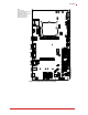
1.2 Major Components (ICs) Table 1-1 lists the major integrated circuits on the LEC-BASE, including a brief description of each IC. Figure 1-2 shows the locations of the major ICs. Table 1-1: Major Integrated Circuit Descriptions and Functions 2 Chip Type Mfg. Model Description Function G-Sensor (U4) Freescale Semicondu ctor MMA7660FC 3-axis Orientation/ Motion Detection Sensor, connected to the I2C GP interface at pins S48 and S49 of the SMARC connector. The I2C address is 0x4C/0x4D.
LEC-BASE Key: U4 - G-Sensor U18 - Touch Panel Controller U19 - I2C EEPROM U25, U26 - CAN Transceivers U27 - Audio CODEC U36 - Real Time Clock U136 - GPS Module U25 U18 U26 U19 U36 U136 U27 LEC-BASE_Top_Comp_b U4 Figure 1-2: Component Locations (Top Side) Overview 3
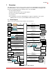
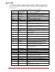
1.3 Interface Headers, Jumper Headers, Switches, LEDs, and Connectors Table 1-2 describes the headers, switches, LEDs, and connectors for the LEC-BASE baseboard shown in Figure 1-3.
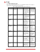
LEC-BASE Table 1-2: Header, Switch, LED, and Connector Descriptions (Continued) JP4 JP5 Battery Charger Enable Cell Charger Present JP6 Cell Charger Voltage JP7 Cell Protection IC, I2C Signal Pair JP8 LCD/LVDS Select (High = 1-2; Low = 2-3) JP9 LCD/LVDS Select (High = 1-2; Low = 2-3) JP10 LVDS JP11 LVDS JP12 JP16 LVDS Backlight Control (for J14) LVDS Panel Control (for J14) LVDS Backlight Control (for J14) I2C Select (related to JP3) Boot Select 0 JP17 Boot Select 1 JP18 Boot Select 2 J
Table 1-2: Header, Switch, LED, and Connector Descriptions (Continued) LED12 LED13 LED14 LED15 LED16 MINIPCIE1 Cell Protection IC Cell Protection IC Cell Protection IC Cell Protection IC Power PCIE Mini Card MINIPCIE2 PCIE Mini Card PC1 PCIE1 TTL Panel Control PCI Express PWM1 PWRON1 PWRON2 Power Management Power On Power On SATA1 SATA SD2 SIM1 SIM2 SPDIF1 SPI0 SD Card Slot SIM Slot SIM Slot SPDIF-OUT Audio System Packet Interface System Packet Interface Reset Switch USB Micro-USB USB SPI1 SW15
LEC-BASE Key: LAN1 - Ehternet LED1 - USB LED2 - Mini PCIE1 LED3 - Mini PCIE2 LED4 - nLID LED5 - nSLEEP LED6 - nBATLOW LED7 - SATA LED8 - SD Card (4 bits) LED9 - USB JP4 LED11 - Cell Protection IC JACK1 LED12 - Cell Protection IC LED13 - Cell Protection IC LED14 - Cell Protection IC CN5 LED15 - Cell Protection IC LED16 - Power MINIPCIE1 - PCIe Mini Card MINIPCIE2 - PCIe Mini Card H25 PC1 - TTL Panel Control PCIE1 - PCI Express PWM1 - Power Management JP7 PWRON1 - Power On JP6 JP5 PWRON2 - Power On SATA1 - S
1.4 Specifications 1.4.1 Physical Specifications Table 1-3 lists the physical dimensions of the baseboard. Table 1-3: Weight and Footprint Dimensions Item Dimension Weight Height (overall) Board thickness Width Length 0.42 kg (0.93 lb) 33.02 mm (1.30 inches) 2.03 mm (0.08 inches) 175.00 mm (6.89 inches) 330.00 mm (12.99 inches) 1.4.2 Overall height is measured from the upper board surface to the top of the highest permanent component on the upper board surface.
LEC-BASE 2 Interface Signals This section provides the pin signals for all the non-standard user interfaces on the LEC-BASE. Signal definitions for standard interfaces such as SATA, USB, PCIe, and DB9 serial connectors can be found in their respective specification data sheets.
Table 2-4: SD/eMMC (AFB2) Interface Pin Signals (Continued) 36 37 38 39 40 41 42 43 44 45 46 47 48 49 50 51 52 53 54 55 56 57 58 59 60 GND GND GND MMC2_D6_3V GND GND GND GND GND MMC2_D7_3V GND GND GND GND GND MMC2_CK_3V GND GND GND GND GND MMC2_CMDD_3V GND GND GND NOTE: The shaded table cells denote power or ground. 2.1.2 Camera 0 (CAM0) Table 2-5 lists the pin signals of the Camera0 header, which provides 10-pins, 2 rows, odd/even pin sequence (1, 2) with 0.079" (2.00mm) pitch.
LEC-BASE 2.1.3 Camera 1 (CAM1) Table 2-6 lists the pin signals of the Camera1 header, which provides 10-pins, 2 rows, odd/even pin sequence (1, 2) with 0.079" (2.00mm) pitch. These signals are connected to the camera control signals at the SMARC connector. Table 2-6: Camera 1 Pin Signals (CAM1) Pin # 1 2 3 4 5 6 7 8 9 10 Signal CSI0_CK+ CSI0_CKCSI0_D0+ CSI0_D0CSI0_D1+ Not Connected CSI0_D1Not Connected GND GND NOTE: The shaded table cells denote ground. 2.1.
2.1.5 Controller Area Network (CAN1) Table 2-8 and Table 2-9 list the pin signals of the Controller Area Network interface (CAN1A and CAN1B), which provides standard dual DB9 connectors. Table 2-8: Controller Area Network Signals (CAN1A) Pin # Signal 1 Not Connected 2 3 CAN1_H Not Connected Not Connected GND Not Connected 4 5 6 7 8 CAN1_L Not Connected 5 Volt 9 NOTE: These pins are connected over the CAN transceiver to the CAN0 SMARC connector interface (pins P143 and P144.
LEC-BASE 2.1.7 GPIO1 Table 2-11 lists the pin signals of the General Purpose IO header, which provides 12 pins in 2 rows, odd/even pin sequence (1, 2), and 0.079" (2.00mm) pitch. These pins are connected to the SMARC connector over the 3.3 volt level shifter.
2.1.9 I2S1 Table 2-13 lists the pin signals of the I2S1 header, which provides 6 pins in a single row with 0.098" (2.50mm) pitch. These pins are connected to the SMARC connector over the 3.3 volt level shifter. Table 2-13: I2S1 Signals (I2S1) Pin # Signal VDD_3V3 1 2 MCBSP1_FSX_3V (connected to SMARC pin S39) MCBSP1_DX_3V (connected to SMARC pin S40) MCBSP1_DR_3V (connected to SMARC pin S41) MCBSP1_CLKX_3V (connected to SMARC pin S42) GND 3 4 5 6 NOTE: Shaded table cells denote power or ground. 2.1.
LEC-BASE 2.1.12 Alternate Function Block 1 (J9) Table 2-16 lists the pin signals of the Alternate Function Block 1 header which provides 34-pins, 2 rows, odd/even pin sequence (1, 2) with 0.079" (2.0mm) pitch. These pins are connected dirctly to the SMARC connector.
2.1.13 I2C (J10) Table 2-17 lists the pin signals of the I2C header, which provides 2 pins with 0.049" (1.25mm) pitch. These pins are connected to the SMARC connector over the 3.3 volt level shifter. Table 2-17: I2C Signals (J10) Pin # I2C_GP_DAT_3V (connected to SMARC pin S48) I2C_GP_CK_3V (connected to SMARC pin S49) 1 2 2.1.14 Signal Battery (J12) Table 2-18 lists the pin signals of the battery header, which provides 2 pins with 0.049" (1.25mm) pitch.
LEC-BASE 2.1.17 Power Management (PW1) Table 2-21 lists the pin signals of the Power Management header, which provides 14 pins in 2 rows, odd/even pin sequence (1, 2), and 0.079" (2.00mm) pitch. These pins are connected directly to the Power Management pins at the SMARC connector.
2.1.20 LVDS Table 2-24 lists the pin signals of the LVDS header which provides 34-pins, 2 rows, odd/even pin sequence (1, 2) with 0.079" (2.0mm) pitch. These pins are connected directly to the LVDS interface at the SMARC connector.
LEC-BASE 2.1.21 TTL Table 2-25 lists the pin signals of the TTL header which provides 34-pins, 2 rows, odd/even pin sequence (1, 2) with 0.079" (2.0mm) pitch. These pins are connected directly to the LCD interface at the SMARC connector.
20 Interface Signals
LEC-BASE Appendix A Technical Support ADLINK Technology, Inc. provides a number of methods for contacting Technical Support listed in Table A-1 below. Requests for support through Ask an Expert are given the highest priorities, and usually will be addressed within one working day. ADLINK Ask an Expert – This is a comprehensive support center designed to meet all your technical needs. This service is free and available 24 hours a day through the ADLINK web site at http://www.adlinktech.com/AAE/.
Table A-1: Technical Support Contact Information (Continued) ADLINK Technology Beijing Address: ࣫ҀᏖ⍋⎔ऎϞഄϰ䏃 1 োⲜ߯ࡼॺ E ᑻ 801 ᅸ(100085) Rm. 801, Power Creative E, No. 1 Shang Di East Rd. Beijing, 100085 China Tel: +86-10-5885-8666 Fax: +86-10-5885-8626 Email: market@adlinktech.com ADLINK Technology Shenzhen Address: ⏅ഇᏖफቅऎ⾥ᡔುफऎ催ᮄफϗ䘧 ᭄ᄫᡔᴃು A1 ᷟ 2 ὐ C ऎ (518057) 2F, C Block, Bldg. A1, Cyber-Tech Zone, Gao Xin Ave. Sec. 7 High-Tech Industrial Park S.
LEC-BASE Table A-1: Technical Support Contact Information (Continued) ADLINK Technology, Inc. (Israeli Liaison Office) Address: 27 Maskit St., Corex Building PO Box 12777 Herzliya 4673300, Israel Tel: +972-54-632-5251 Fax: +972-77-208-0230 Email: israel@adlinktech.com ADLINK Technology, Inc. (UK Liaison Office) Tel: +44 774 010 59 65 Email: UK@adlinktech.
24