LEC‐BTS (Computer‐on‐Module) Technical Reference P/N 50‐1Z173‐1000 Rev 1.0 Advance Technologies. Automate the World.
Disclaimer Information in this document is provided in connection with ADLINK products. No license, express or implied, by estoppel or otherwise, to any intellectual property rights is granted by this document.
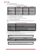
LEC-BTS Table of Contents 1 Overview ........................................................................................................................... 1 1.1 Block Diagram........................................................................................................................ 1 1.2 Major Components (ICs)........................................................................................................ 2 1.3 Connectors, Switches, and LEDs ...................................
iv
LEC-BTS 1 Overview This initial manual version presents a general overview of the LEC-BTS. After reviewing this document you should understand the following features of the LEC-BTS. Functional Block Diagram Major Component (IC) Locations and Descriptions Connector, Switch, and LED Locations and Descriptions Specifications SMARC Interface Signal Definitions and Debug Interface Signal Definitions NOTE: Refer to http://www.sget.org/standards/smarc.html for SMARC specifications.
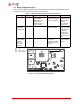
1.2 Major Components (ICs) Table 1-1 lists the major integrated circuits on the LEC-BTS, including a brief description of each IC. Figures 1-2 and 1-3 show the locations of the major ICs. Table 1-1: Major Integrated Circuit Descriptions and Functions Chip Type Mfg. Model CPU (U1) Intel Ethernet Controller (U9 [bottom]) Intel E3815 (single core, 5W, 1.46GHz) E3826 (dual core, 7W, 1.46GHz) E3845 (quad core, 10W, 1.
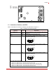
LEC-BTS Key: U9 - GbE Controller U24 - DDR3L SDRAM U27 - DDR3L SDRAM U27 U9 S158 LEC_BTS_Bot_Comp_a U24 S75 Figure 1-3: Component Locations (Bottom Side) 1.3 Connectors, Switches, and LEDs Table 1-2 describes the connectors, switches, and LEDs shown in Figure 1-4. Table 1-2: Module Connector Description Reference GF1 – SMARC P-S CN1 SW1 Board Access Top/ Bottom Top Top Description 314-pin, MXM edge connector for Memory, Video, and I/O functions.
Table 1-2: Module Connector Description (Continued) SW4 Top 4-pin dip switch for loading BIOS setup defaults at Boot Up: 1 = 18bit [default] 4 = 24bit 2 = off [default] 3 = on and selecting 18/24 bit LVDS modes SW5 Top (1 2) LEC-BT_SW4_b 12 ON (4 3) Switch Default Setting 4-pin dip switch for BIOS_SELECT: 1 = BIOS 2 [blue LED blinks fast] 4 = BIOS 1 and WDT Disable [default] 2 = BMC switches to BIOS 2 when BIOS 1 not detected [default] 3 = Disables BIOS Detection Watchdog LED1 Top LED2 LED3 T
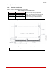
LEC-BTS 1.4 Specifications 1.4.1 Physical Specifications Table 1-3 lists the physical dimensions of the module. Table 1-3: Weight and Footprint Dimensions Item Weight Height (overall) Board thickness Width Length 0.02 kg (0.05 lb) 2.50 mm (0.098 inches) 1.27 mm (0.05 inches) 50.00 mm (1.97 inches) 82.00 mm (3.23 inches) Overall height is measured from the upper board surface to the top of the highest permanent component (CN1 connector) on the upper board surface.
1.4.3 Power Specifications Table 1-4 provides the power requirements for this module.
LEC-BTS 2 Hardware 2.1 CPU The LEC-BTS product family offers three versions of the Intel Atom E3800 Series CPU: the E3815 (Single Core), the E3826 (Dual Core), and the E3845 (Quad Core). E3800 CPUs feature the Intel 64 Architecture and are manufactured based on Intel’s 22-nanometer technology. Refer to the CPU data sheet at: http://www.intel.com/content/dam/www/public/us/en/documents/datasheets/atom-e3800-family-datasheet.pdf 2.2 Memory The LEC-BTS employs one channel of 64-bit DDR3L on-board memory.
3.1 18/24 Bit LVDS LCD The LVDS interface is connected to the DDI0 interface of the SoC, while the translation is made by a DisplayPort™-to-LVDS converter. (Refer to the Realtek RTD2136R-CG, DisplayPort-to-LVDS converter datasheet.) NOTE: Backlight Enable, Display Enable, and PWMOUT are controlled from the BIOS setup. 3.
LEC-BTS 3.10 SPI The CPU implements an SPI controller, which supports two SPI Flash devices on the module for BIOS storage. 3.11 Serial (UART) The LEC-BTS provides three serial interfaces: Two ports are high-speed, 4-wire ports (with TX/ RX and RTS#/CTS#), and one port is 2-wire (with TX/RX only.) 3.12 I2S The SMARC connector provides three pins for an LPE_I2S audio interface. The LPE_I2S interface is brought out through the I2S0 pins on the SMARC connector. 3.
3.17 SMARC Interface Signals Table 3-2 provides the pin signals for the SMARC P-S connector. Refer to the SMARC specification at http://www.sget.org/standards/smarc.html for definitions of the SMARC signals.
LEC-BTS Table 3-2: SMARC P-S Connector (GF1) Signal Descriptions (Continued) P43 P44 P45 P46 P47 P48 P49 P50 P51 P52 P53 P54 P55 P56 P57 P58 P59 P60 P61 P62 P63 P64 P65 P66 P67 P68 P69 P70 P71 P72 P73 P74 P75 P76 P77 P78 P79 P80 P81 P82 P83 P84 P85 P86 P87 P88 P89 P90 P91 P92 Interfaces Not connected Not connected Not connected Not connected GND SATA0_TX+ SATA0_TXGND SATA_RX+ SATA_RXGND SPI1_CS0# Not connected SPI1_CK SPI1_DIN SPI1_DO GND USB0+ USB0USB0_EN_OC# Not connected Not connected USB1+ USB1USB1_EN_
Table 3-2: SMARC P-S Connector (GF1) Signal Descriptions (Continued) P93 P94 P95 P96 P97 P98 P99 P100 P101 P102 P103 P104 P105 P106 P107 P108 P109 P110 P111 P112 P113 P114 P115 P116 P117 P118 P119 P120 P121 P122 P123 P124 P125 P126 P127 P128 P129 P130 P131 P132 P133 P134 P135 P136 P137 12 HDMI_D2GND HDMI_D1+ HDMI_D1GND HDMI_D0+ HDMI_D0GND HDMI_CK+ HDMI_CKGND HDMI_HPD HDMI_CTRL_CK HDMI_CTRL_DAT HDMI_CEC GPIO0 / CAM0_PWR# [default] GPIO1 / CAM1_PWR# [default] GPIO2 / CAM0_RST# [default] GPIO3 / CAM1_RST# [d
LEC-BTS Table 3-2: SMARC P-S Connector (GF1) Signal Descriptions (Continued) P138 P139 P140 P141 P142 P143 P144 P145 P146 P147 P148 P149 P150 P151 P152 P153 P154 P155 P156 SER2_RTS# SER2_CTS# Not connected Not connected GND Not connected Not connected Not connected Not connected VDD_IN VDD_IN VDD_IN VDD_IN VDD_IN VDD_IN VDD_IN VDD_IN VDD_IN VDD_IN S139 S140 S141 S142 S143 S144 S145 S146 S147 S148 S149 S150 S151 S152 S153 S154 S155 S156 S157 S158 I2C_LCD_CK I2C_LCD_DAT LCD_BKLT_PWM Not connected GND RSVD
Table 3-3: Debug Interface Signals (CN1) (Continued) 25 26 27 28 29 30 31 32 33 34 35 36 37 38 39 40 LPC_AD1 LPC_AD2 LPC_AD3 LPC_FRAME# CLK33_LPC RST# BIOS_DIS0 GND2 LPC_3V3 SPI_BIOS_CLK SPI_BIOS_MOSI SPI_BIOS_MISO SPI_BIOS_CS1# SPI_BIOS_CS0# GND1 VCC_SPI_IN NOTE: The gray table cells denote ground.
LEC-BTS Appendix A Technical Support ADLINK Technology, Inc. provides a number of methods for contacting Technical Support listed in Table A-1 below. Requests for support through Ask an Expert are given the highest priorities, and usually will be addressed within one working day. ADLINK Ask an Expert – This is a comprehensive support center designed to meet all your technical needs. This service is free and available 24 hours a day through the ADLINK web site at http://www.adlinktech.com/AAE/.
Table A-1: Technical Support Contact Information (Continued) ADLINK Technology Beijing Address: ࣫ҀᏖ⍋⎔ऎϞഄϰ䏃 1 োⲜ߯ࡼॺ E ᑻ 801 ᅸ(100085) Rm. 801, Power Creative E, No. 1, Shang Di East Rd., Beijing, 100085 China Tel: +86-10-5885-8666 Fax: +86-10-5885-8626 Email: market@adlinktech.com ADLINK Technology Shenzhen Address: ⏅ഇᏖफቅऎ⾥ᡔುफऎ催ᮄफϗ䘧 ᭄ᄫᡔᴃು A1 ᷟ 2 ὐ C ऎ (518057) 2F, C Block, Bldg. A1, Cyber-Tech Zone, Gao Xin Ave. Sec. 7, High-Tech Industrial Park S.
LEC-BTS Table A-1: Technical Support Contact Information (Continued) ADLINK Technology, Inc. (Israeli Liaison Office) Address: 27 Maskit St., Corex Building PO Box 12777 Herzliya 4673300, Israel Tel: +972-77-208-0230 Fax: +972-77-208-0230 Email: israel@adlinktech.com ADLINK Technology, Inc. (UK Liaison Office) Tel: +44 774 010 59 65 Email: UK@adlinktech.
18