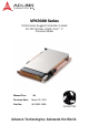
VPX3000 Series Performance Rugged Conduction Cooled 3U VPX 3rd Gen Intel® Core™ i7 Processor Blade Manual Rev.: 1.00 Revision Date: March 29, 2013 Part No: 50-15092-1000 Advance Technologies; Automate the World.
Revision History Revision Release Date 1.
VPX3000 Preface Copyright 2013 ADLINK Technology Inc. This document contains proprietary information protected by copyright. All rights are reserved. No part of this manual may be reproduced by any mechanical, electronic, or other means in any form without prior written permission of the manufacturer. Disclaimer The information in this document is subject to change without prior notice in order to improve reliability, design, and function and does not represent a commitment on the part of the manufacturer.
Using this Manual Audience and Scope The VPX3000 User’s Manual is intended for hardware technicians and systems operators with knowledge of installing, configuring and operating industrial grade computer systems. Manual Organization This manual is organized as follows: Chapter 1, Introduction: Introduces the VPX3000, its features, block diagrams, and package contents. Chapter 2, Specifications: Presents detailed specification information.
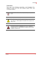
VPX3000 Conventions Take note of the following conventions used throughout this manual to make sure that users perform certain tasks and instructions properly. Additional information, aids, and tips that help users perform tasks. NOTE: CAUTION: WARNING: Preface Information to prevent minor physical injury, component damage, data loss, and/or program corruption when trying to complete a task.
This page intentionally left blank.
VPX3000 Table of Contents Revision History...................................................................... ii Preface .................................................................................... iii List of Figures ........................................................................ ix List of Tables.......................................................................... xi 1 Introduction ........................................................................ 1 1.1 Overview...........
4.4 VPX-R300 RTM Board Layout........................................... 26 4.5 VPX-R300 RTM Connector Pin Assignments.................... 27 4.6 Switches............................................................................. 34 Important Safety Instructions............................................... 35 Getting Service ......................................................................
VPX3000 List of Figures Figure 1-1: Figure 1-2: Figure 1-3: Figure 4-1: Figure 4-2: Figure 4-3: VPX3000 Functional Block Diagram................................ 3 VPX-R300 RTM Functional Block Diagram ..................... 4 tBP-VPX3000 Test Backplane Functional Block Diagram5 VPX3000 Board Layout ................................................. 19 VPX3000 Mechanical Drawing ...................................... 20 VPX-R300 RTM Board Layout.......................................
This page intentionally left blank.
VPX3000 List of Tables Table 2-1: VPX3000 Blade Specifications ........................................ 9 Table 2-2: VPX-R300 RTM Specifications......................................
This page intentionally left blank.
VPX3000 1 Introduction 1.1 Overview The VPX3000 Series is a 3U VPX processor blade featuring the 3rd Generation Intel® Core i7 processor with Mobile Intel® QM77 Express Chipset. The VPX3000 provides up to 8GB DDR3-1066/1333 dual channel ECC memory soldered onboard, one PCI Express x8 XMC.3 site with VITA 46.9 rear IO, and onboard soldered 16GB SLC SATA solid state drive. Rear I/O via P1 and P2 includes 1000BASE-T, HD Audio (Line-in, Line-out), 2x SATA 6 Gb/s, 1x SATA 3 Gb/s, USB 3.0, USB 2.
1.2 Features 2 X 3U VPX VITA 46, OpenVPX VITA 65, VPX REDI 48 X 4HP (0.8") rugged conduction cooled 3U VPX blade with conformal coating X Intel® 3rd generation Core™ i7-3612QE Processor (4 cores, 6M cache, 2.1 GHz, 35W TDP) X Dual channel DDR3-1333/1666 SDRAM with ECC soldered onboard, up to 8GB X Intel® QM77 PCH X Intel® HD Graphics 4000 with DX11, OpenGL 3.1 and OCL 1.1 X Onboard PCI Express x8 XMC site with VITA 46.
VPX3000 1.3 Block Diagrams IMVP7 Vcore PCIe2.0x8 or PCIe2.0x4 + PCIe2.0x4 PCIe switch PEX8619 Intel® Core™ i7 A On Board ECC Max 512MBX8 B On Board ECC Max 512MBX8 quad/dual-core SV-BGA PCIE[8..15] XMC PCIE[0..7] PCIe2.0x8 GPIO 0,1,2* X8d+X12d SATA Gen3 Port 0,1 VGA RS-422** P2 HDA ALC262 FDI Line-in, Line-out DMI P1 USB 3.0 Port 0 and USB 2.0 Port 0, 6 UART D** 1000 BASE-T GPIO 3** 1000 BASE-BX 1000 BASE-BX DVI GbE Intel 82580EB PCIe2.
VS1(DC12V), 8A/slot VS2(DC3V), 8A/slot VS3(DC5V), 16A/slot DC3V_AUX,1A/Slot RP0 DC12V_AUX,1A/Slot DC-12V_AUX,1A/Slot VBAT NVMRO, SYSRESET# SATA 0 ~ SATA 1 SATA3.0 2 port USB 2.0 USB2.0 1 port USB3.0 +USB2.0 USB3.
VPX3000 Slot#1 Slot#2 Slot#3 VS1(DC12V), 32A/slot VS2(DC3V), 32A/slot VS3(DC5V), 23A/slot DC3V_AUX,1A/Slot DC12V_AUX,1A/Slot DC-12V_AUX,1A/Slot REF_CLK+/SM[0:1] IPM2, SM[2:3] I2C NVMRO, SYSRESET#, JTAG VBAT 2x PCIe by 4 1000BASE-BX Crossover Crossover 2x PCIe by 4 2x PCIe by 4 PCIE8~PCIE15 2x GbE 1000BASE-BX 1000BASE-BX PCIE x4 2 Slots 4xSMA LAN 10/100/1000BASE-T 1000BASE-T 1000BASE-T RJ-45 jack SATA 0 ~ SATA 1 SATA3.0 2 port USB 2.0 USB2.0 1 port USB3.0 +USB2.0 USB3.
1.
VPX3000 1.5 Package Contents The VPX3000 is packaged with the following components. If any of the items on the contents list are missing or damaged, retain the shipping carton and packing material and contact the dealer for inspection. Please obtain authorization before returning any product to ADLINK. The packing contents of the VPX3000 are non-standard configurations and may vary depending on customer requests.
This page intentionally left blank.
VPX3000 2 Specifications 2.1 VPX3000 Blade Specifications VITA Standards • • • • VITA 46.0 VPX Base Standard VITA 46.4 PCI Express on VPX Fabric Connector VITA 46.6 Gigabit Ethernet Control Plane on VPX VITA 46.9 PMC/XMC/Ethernet Signal Mapping to 3U/6U VPX • VITA 46.11(draft) System Management on VPX • VITA 48.0 Ruggedized Enhanced Design Implementation Mechanical Base Specification • VITA 65 OpenVPX Architecture Framework for VPX Mechanical • IEEE 1101.
XMC • One PCIe 2.0 x8 conduction cooled XMC.3 site • Jn6 rear XMC I/O connector compliant to VITA 46.9, X8d+X12d Front Panel I/O • Reset button • Power LED Storage Interfaces1 • Onboard SATA NAND flash on SATA 3 Gb/s, up to 32GB • SATA 6 Gb/s port 0 and 1 to P1 • SATA 3 Gb/s port 2 to P2 BIOS • AMI EFI BIOS, 64Mbit SPI flash memory P1 Interface • • • • • • • Line-in Line-out 2x SATA 6 Gb/s ports 2x USB 2.0 USB 3.
VPX3000 2.2 VPX-R300 RTM Specifications VITA Standards • VITA 46.10 Rear Transition Module on VPX Mechanical • 100mm x 80mm Faceplate I/O • • • • DVI-I port USB 2.0 port USB 3.0 port 10/100/1000BASE-T Ethernet port Onboard Interfaces • • • • • • • • Line-in audio jack Line-out audio jack RS-232 (RJ-45) RS-422 (RJ-45) 2x SATA 3.0 ports 8x pin headers for GPIO XMC port 4x status LEDs for GPIO Table 2-2: VPX-R300 RTM Specifications Note: Specifications are subject to change without prior notice.
2.
VPX3000 3 Functional Description The following sections describe the VPX3000 features and functions. 3.1 Processors The 3rd Generation Intel® Core™ i7 Processor is the next generation of 64-bit, multi-core mobile processors built on 22-nanometer process technology. Based on a new micro-architecture, the processor is designed for a two-chip platform. The two-chip platform consists of a processor and Platform Controller Hub (PCH).
Supported Technologies Z Intel® Virtualization Technology for Directed I/O (Intel® VT-d) X Intel® Virtualization Technology (Intel® VT-x) X Intel® vPro Technology (Intel® VT) X Intel® Trusted Execution Technology (Intel® TXT) X Intel® Hyper-Threading Technology X Intel® 64 Architecture X Intel® Turbo Boost Technology 2.
VPX3000 3.2 Chipset The VPX3000 incorporates the Mobile Intel® QM77 Express Chipset (Intel® BD82QM77 PCH). Mobile Intel® QM77 Express Chipset X PCI Express Base Specification, Revision 2.0 support for up to eight ports with transfer rate up to 5 GT/s X Supports dual display X ACPI Power Management Logic Support, Revision 4.0a X Enhanced DMA controller, interrupt controller, and timer functions X Integrated Serial ATA host controllers with independent DMA operation on up to six ports and SATA 6.
3.3 Intel® Turbo Boost Technology Intel Turbo Boost Technology is a feature that allows the processor to opportunistically and automatically run faster than its rated operating core and/or render clock frequency when there is sufficient power headroom, and the product is within specified temperature and current limits. The Intel Turbo Boost Technology feature is designed to increase performance of both multi-threaded and single-threaded workloads.
VPX3000 3.5 PMC/XMC Site The VPX3000 Series supports one XMC site for rear I/O expansion. The XMC site provides a x8 PCI Express 2.0 lane. Jn6 rear XMC I/O connector is compliant to VITA 46.9, X8d+X12d. 3.6 Real Time Clock The Intel® QM77 PCH contains a Motorola MC146818B-compatible real-time clock (RTC) with 256 bytes of RAM. The real-time clock performs two key functions: keeping track of the time of day and storing system data. The RTC operates on a 32.
This page intentionally left blank.
VPX3000 4 Board Interfaces (1.6) 4.1 VPX3000 Board Layout (160) LAN P0 (99.
4.2 VPX3000 Mechanical Drawing 160 99.85 Power LED 14.34 4.6 18.
VPX3000 4.3 VPX3000 Connector Pin Assignments XMC Connectors F1 F19 A1 A19 JN1 Connector Pin A B C D E F 1 RXP0 RXN0 +3.3V RXP1 RXN1 VPWR 2 GND GND TRST# GND GND MRSTI# 3 RXP2 RXN2 +3.3V RXP3 RXN3 VPWR 4 GND GND TCK GND GND MRSTO# 5 RXP4 RXN4 +3.3V RXP5 RXN5 VPWR 6 GND GND TMS GND GND +12V 7 RXP6 RXN6 +3.
JN2 Connector Pin A B C D E F 1 JN6_A1 JN6_B1 NC JN6_D1 JN6_E1 NC 2 GND GND NC GND GND NC 3 JN6_A3 JN6_B3 NC JN6_D3 JN6_E3 NC 4 GND GND NC GND GND NC 5 JN6_A5 JN6_B5 NC JN6_D5 JN6_D6 NC 6 GND GND NC GND GND NC 7 JN6_A7 JN6_B7 NC JN6_D7 JN6_D7 NC 8 GND GND NC GND GND NC 22 9 JN6_A9 JN6_B9 NC JN6_D9 JN6_D9 NC 10 GND GND NC GND GND NC 11 JN6_A11 JN6_B11 NC JN6_D11 JN6_D11 NC 12 GND GND NC GND GND NC 13 JN6_A13 JN6_B13
VPX3000 VPX Connectors P0 Connector Pin G F E D C B A 1 +12V +12V +12V None +3.3V +3.3V +3.3V 2 +12V +12V +12V None +3.3V +3.3V +3.3V 3 +5V +5V +5V None +5V +5V +5V 4 I2C_CLK I2C_DAT GND +12V_AUX GND SYSRESET NC 5 GAP GA4 GND +3.
P1 Connector Pin G F E D C B A 1 NC GND L0-TX- L0-TX+ GND L0-RX- L0-RX+ 2 GND L1-TX- L1-TX+ GND L1-RX- L1-RX+ GND 3 VBAT GND L2-TX- L2-TX+ GND L2-RX- L2-RX+ 4 GND L3-TX- L3-TX+ GND L3-RX- L3-RX+ GND 5 SYSCON# GND L4-TX- L4-TX+ GND L4-RX- L4-RX+ 6 GND L5-TX- L5-TX+ GND L5-RX- L5-RX+ GND 7 NC GND L6-TX- L6-TX+ GND L6-RX- L6-RX+ 8 GND L7-TX- L7-TX+ GND L7-RX- L7-RX+ GND 9 GPIO1 GND SATA0-TX- SATA0-TX+ GND SATA0-RX- SATA0-RX+ 10 GN
VPX3000 P2 Connector Pin G F E D C B A 1 GPIO3 GND DVI_TX1- DVI_TX1+ GND DVI_TX0- DVI_TX0+ 2 GND DVI_TXC- DVI_TXC+ GND DVI_TX2- DVI_TX2+ GND 3 VGA_SDA GND NC DVI_HPD GND DVI_SCL DVI_SDA 4 GND COM_SIN COM_SOUT GND COM_CTS# COM_RTS# GND 5 VGA_SCL GND RS422_TX- RS422_TX+ GND RS422_RX- RS422_RX+ 6 GND Linein-L Linein-R AGND Lineout-L Lineout-R AGND 7 VGA-HS GND J16-A1 J16-B1 GND J16-D1 J16-E1 8 GND J16-A3 J16-B3 GND J16-D3 J16-E3 GND 9 VG
4.4 VPX-R300 RTM Board Layout (83.5) (20) AP1 CN11 CN9 (99.85) CN1 CN12 CN8 CN10 CN4 CN5 CN7 CN2 CN15 CN3 CN13 CN6 AP2 CN1 VPX Connector RP0 CN8 DVI-I port CN2 VPX Connector RP1 CN9 Line-in Port CN3 VPX Connector RP2 CN10 Line-out Port AP1/2 Alignment keys CN11 RS-232 Port CN4/5 7-pin SATA connectors CN12 RS-422 Port CN6 USB 3.0 port CN13 XMC connector CN7 USB 2.
VPX3000 4.5 VPX-R300 RTM Connector Pin Assignments Rear I/O Connectors Gigabit Ethernet Connectors (CN11, RJ-45) Pin # GbE Signal 1 MX0+ 2 MX0- 3 MX1+ 4 MX2+ 5 MX2- 6 MX1- 7 MX3+ 8 MX3- 8 1 USB 2.
USB 3.
VPX3000 Onboard Connectors SATA Connector (CN12/13) Pin # Signal 1 2 3 4 5 6 7 GND TXP TXN GND RXN RXP GND 1 2 3 4 5 6 7 RS-232 (CN31, RJ-45) Pin # RS-232 1 N.C. 2 S3_RTS-L(RTS) 3 N.C. 4 S3_SOUT(TXD) 5 S3_SIN(RXD) 6 GND. 7 S3_CTS-L(CTS) 8 N.C. 8 1 8 1 RS-422 (CN32, RJ-45) Board Interfaces Pin # RS-232 1 S3_TXD422- 2 N.C. 3 N.C. 4 S3_RXD422+ 5 S3_TXD422+ 6 GND 7 N.C.
XMC Connector (CN36) F1 F19 A1 A19 Pin A B C D E F 1 +5V S3_JN6-E1 2 NC GND S3_JN6-D1 +3.3V S3_JN6-B1 S3_JN6-A1 GND TRST# GND 3 +5V GND S3_JN6-E3 S3_JN6-D3 +3.3V S3_JN6-B3 S3_JN6-A3 4 NC GND GND TCK GND GND 5 +5V S3_JN6-E5 S3_JN6-D5 +3.3V S3_JN6-B5 S3_JN6-A5 6 +12V GND GND TMS GND GND 7 +5V S3_JN6-E7 S3_JN6-D7 +3.3V S3_JN6-B7 S3_JN6-A7 8 -12V GND GND TDI GND GND S3_JN6-A9 9 +5V S3_JN6-E9 S3_JN6-D9 +3.
VPX3000 RTM VPX Connectors RP0 Connector Pin G F E D C B A 1 +12V +12V +12V +12V NC +3.3V +3.3V 2 +12V +12V +12V +12V NC +3.3V +3.3V 3 +5V +5V +5V +5V NC +5V +5V 4 SM2 SM3 GND -12V_AUX GND SYSRESET NVMRO 5 GAP* GA4* GND 3.
RP1 Connector Pin G F E D C B A 1 GPIO0 GND NC NC GND NC NC GND 2 GND NC NC GND NC NC 3 GPIO1 GND NC NC GND NC NC 4 GND NC NC GND NC NC GND 5 GPIO2 GND MDIN1 MDIP1 GND MDIN0 MDIP0 6 GND MDIN3 MDIP3 GND MDIN2 MDIP2 GND 7 Maskreset GND NC NC GND NC NC 8 GND NC NC GND NC NC GND 9 GPIO3 GND DVI_TX1- DVI_TX1+ GND DVI_TX0- DVI_TX0+ 10 GND DVI_TXC- DVI_TXC+ GND DVI_TX2- DVI_TX2+ GND 11 VGA_SDA GND ? DVI_HPD GND DVI_SCL DV
VPX3000 RP2 Connector Pin G F E D C B A 1 VGA-VS GND J16-A11 J16-B11 GND J16-D11 J16-E11 2 GND J16-A13 J16-B13 GND J16-D13 J16-E13 GND 3 VGA-R GND J16-A5 J16-B5 GND J16-D5 J16-E5 4 GND J16-A7 J16-B7 GND J16-D7 J16-E7 GND 5 VGA-B GND J16-A9 J16-B9 GND J16-D9 J16-E9 6 GND J16-A15 J16-B15 GND J16-D15 J16-E15 GND 7 VGA-G GND J16-A17 J16-B17 GND J16-D17 J16-E17 8 GND J16-A19 J16-B19 GND J16-D19 J16-E19 GND Board Interfaces 33
4.6 Switches PCI Express to P1 Configuration Switch (SW) This switch sets the PCI Express Lane configuration at the P1 connector.
VPX3000 Important Safety Instructions For user safety, please read and follow all instructions, WARNINGS, CAUTIONS, and NOTES marked in this manual and on the associated equipment before handling/operating the equipment. X Read these safety instructions carefully. X Keep this user’s manual for future reference. X Read the specifications section of this manual for detailed information on the operating environment of this equipment.
X Never attempt to fix the equipment. Equipment should only be serviced by qualified personnel. A Lithium-type battery may be provided for uninterrupted, backup or emergency power. WARNING: X 36 Risk of explosion if battery is replaced with one of an incorrect type. Dispose of used batteries appropriately.
VPX3000 Getting Service Contact us should you require any service or assistance. ADLINK Technology, Inc. Address: 9F, No.166 Jian Yi Road, Zhonghe District New Taipei City 235, Taiwan ᄅؑקխࡉ৬ԫሁ 166 ᇆ 9 ᑔ Tel: +886-2-8226-5877 Fax: +886-2-8226-5717 Email: service@adlinktech.com Ampro ADLINK Technology, Inc. Address: 5215 Hellyer Avenue, #110, San Jose, CA 95138, USA Tel: +1-408-360-0200 Toll Free: +1-800-966-5200 (USA only) Fax: +1-408-360-0222 Email: info@adlinktech.com ADLINK Technology (China) Co.
ADLINK Technology, Inc. (French Liaison Office) Address: 15 rue Emile Baudot, 91300 Massy CEDEX, France Tel: +33 (0) 1 60 12 35 66 Fax: +33 (0) 1 60 12 35 66 Email: france@adlinktech.com ADLINK Technology Japan Corporation Address: ͱ101-0045 ᵅҀ䛑गҷ⬄ऎ⼲⬄䤯 ⬎ފ3-7-4 ⼲⬄ 374 ɛɳ 4F KANDA374 Bldg. 4F, 3-7-4 Kanda Kajicho, Chiyoda-ku, Tokyo 101-0045, Japan Tel: +81-3-4455-3722 Fax: +81-3-5209-6013 Email: japan@adlinktech.com ADLINK Technology, Inc.