
User's Manual
ACM1281 NFC Reader Module Reference Information
info@acs.com.hk
1.00
www.acs.com.hk
Page 5 of 7
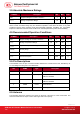
3.0. Absolute Maximum Ratings
SYMBOL Description Min Max Units
VDD Support Voltage to J7’s Pin 1 and Pin 4 4 6 V
T
amb,abs
Storage Temperature Range -40 85
℃
Stress beyond those listed under the Absolute Maximum Ratings may cause permanent damage to
device. These are stress ratings only and functional operation of the device at these or any other
conditions beyond those indicated under Recommended Operating Conditions are not implied.
Exposure to absolute‐maximum‐rated conditions for extended periods may affect device reliability
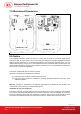
4.0. Recommended Operation Conditions
SYMBOL Description Min Normal
Max Units
VDD Support Voltage to J7’s Pin 1 and Pin 4 4.75 5 5.25 V
T
storage
Storage Temperature Range -10 25 60
℃
T
operation
Operation Temperature Range 0 25 50
℃
Humidity
Humidity Range
- - 90
%
F
c
Carrier Frequency Range
13.553
13.56 13.567
MHz
I
operation
Current Consumption
- 100 200
mA
5.0. Pin Descriptions
The ACM1281 has a five pins connector interface between the module and the host, identified by ref
J7. Pins assignment are given in the table below
PIN NAME Type Description
1 UVCC Power Supply Voltage
2 D- Input/output Differential data lines that conform to the
USB v2.0 standard
3 D+ Input/output Differential data lines that conform to the
USB v2.0 standard
4 UGND Power Power Ground
5 GND Power Shielding Ground
6.0. Antenna
The integrated antenna is etched in the copper on the layer 2 and layer 3 of the circuit board. The
antenna consists of three loops of 0.03” wide copper with 0.03” spacing.