
User`s manual
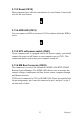
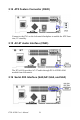


Table Of Contents
- Contents
- Chapter 1 Hardware Configuration
- Chapter 2 Connecting Peripherals
- 2.1 Introduction
- 2.2 1st (CN1) IDE Connectors
- 2.3 Floppy Drive Connector (CN3)
- 2.4 Parallel Port (CN4)
- 2.5 USB Ports (CN6,CN63,CN66,CN67)
- 2.6 VGA Connector CN7
- 2.7 DVI Connector VCN1 (optional)
- 2.8 Ethernet Connector (CN24)
- 2.9 Serial Ports (COM1: CN9/CN91; COM2: CN10 )
- 2.10 PS/2 Keyboard/Mouse Connector (CN11)
- 2.11 External Keyboard Connector (CN12)
- 2.12 CPU Fan Connector (CN68)
- 2.13 Front Panel Connectors (CN16, 17, 18, 19, 21&29)
- 2.14 ATX Feature Connector (CN20)
- 2.15 AC-97 Audio Interface (CN43)
- 2.16 Serial ATA Interface (SA0,SA1,SA2, and SA3)
- 2.17 Connecting to SNMP-1000 Remote Manager
- 2.18 Auxiliary 4-pin Power Connector (ATX1)
- 2.19 SCSI Daughterboard Extension Connector (CN30)
- 2.20 Case Open Connector (CN64)
- 2.21 Front Panel LAN Indicator Connector (CN65)
- 2.22 GPIO Pin Header (CN93)
- Chapter 3 Award BIOS Setup
- 3.1 Introduction
- 3.2 Entering Setup
- 3.3 Standard CMOS Setup
- 3.4 Advanced BIOS Features
- Figure 3.3: Advanced BIOS features screen
- 3.4.1 CPU Features
- 3.4.2 Hard Disk Boot Priority
- 3.4.3 Virus Warning
- 3.4.4 CPU L1 & L2 Cache
- 3.4.5 Hyper-Threading Technology
- 3.4.6 Quick Power On Self Test
- 3.4.7 First/Second/Third Boot Device
- 3.4.8 Boot Other Device
- 3.4.9 Swap Floppy Drive
- 3.4.10 Boot Up Floppy Seek
- 3.4.11 Boot Up NumLock Status
- 3.4.12 Gate A20 Option
- 3.4.13 Typematic Rate Setting
- 3.4.14 Typematic Rate (Chars/Sec)
- 3.4.15 Typematic Delay (msec)
- 3.4.16 Security Option
- 3.4.17 APIC Mode
- 3.4.18 MPS Version Control For OS
- 3.5 Advanced Chipset Features
- Figure 3.4: Advanced chipset features screen
- 3.5.1 DRAM Timing Selectable
- 3.5.2 CAS Latency Time
- 3.5.3 DRAM RAS# to CAS# Delay
- 3.5.4 DRAM RAS# Precharge
- 3.5.5 Precharge Delay (t RAS)
- 3.5.6 System Memory Frequency
- 3.5.7 System BIOS Cacheable
- 3.5.8 Video BIOS Cacheable
- 3.5.9 Memory Hole At 15M-16M
- 3.5.10 PCI-Express Root Port Func
- 3.5.11 On-Chip Video Memory Size
- 3.5.12 On-Chip Frame Buffer Size
- 3.5.13 FIXED Memory Size
- 3.5.14 DVMT Memory Size
- 3.5.15 Init Display First
- 3.6 Integrated Peripherals
- Figure 3.5: Integrated peripherals
- Figure 3.6: On-Chip IDE Device
- 3.6.1 IDE HDD Block Mode
- 3.6.2 IDE DMA Transfer Access
- 3.6.3 On-Chip IDE Device
- 3.6.4 SATA Mode
- 3.6.5 On-Chip Serial ATA
- 3.6.6 PATA IDE Mode
- 3.6.7 SATA Port
- Figure 3.7: Onboard Device
- 3.6.8 USB Controller
- 3.6.9 USB 2.0 Controller
- 3.6.10 USB Keyboard/Mouse Support
- 3.6.11 AC97 Audio
- 3.6.12 Onboard LAN1 Control
- 3.6.13 Onboard LAN2 Control
- 3.6.14 GPIO Function
- Figure 3.8: Super I/O Device
- 3.6.15 KBC Input Clock
- 3.6.16 Onboard FDC Controller
- 3.6.17 Onboard Serial Port 1
- 3.6.18 Onboard Serial Port 2
- 3.6.19 UART Mode Select
- 3.6.20 RxD, TxD Active
- 3.6.21 IR Transmission Delay
- 3.6.22 UR2 Duplex Mode
- 3.6.23 Use IR Pins
- 3.6.24 Onboard Parallel Port
- 3.6.25 Parallel Port Mode
- 3.6.26 EPP Mode Select
- 3.6.27 ECP Mode Use DMA
- 3.7 Power Management Setup
- Figure 3.9: Power management setup screen (1)
- 3.7.1 Power Supply Type
- 3.7.2 ACPI Function
- 3.7.3 Power Management
- 3.7.4 Video Off Method
- 3.7.5 Video Off In Suspend
- 3.7.6 Suspend Type
- 3.7.7 Modem Use IRQ
- 3.7.8 Suspend Mode
- 3.7.9 Soft-Off by PWR-BTTN
- 3.7.10 CPU THRM-Throttling
- 3.7.11 PowerOn by Modem
- 3.7.12 PowerOn by LAN
- 3.7.13 PowerOn by Alarm
- 3.7.14 Primary IDE 0 (1) and Secondary IDE 0 (1)
- 3.7.15 FDD, COM, LPT PORT
- 3.7.16 PCI PIRQ [A-D]#
- 3.7.17 PWRON After PWR-Fail
- 3.8 PnP/PCI Configurations
- 3.9 PC Health Status
- 3.10 Frequency / Voltage Control
- 3.11 Password Setting
- 3.12 Save & Exit Setup
- 3.13 Exit Without Saving
- Chapter 4 Chipset Software Install Utility
- Chapter 5 VGA Setup
- Chapter 6 LAN Configuration
- Chapter 7 USB 2.0 Configuration
- Chapter 8 Onboard Security Setup
- Appendix A Programming the watchdog
- Appendix B Programming the GPIO
- Appendix C Pin Assignments
- C.1 IDE Hard Drive Connector (CN1)
- C.2 Floppy Drive Connector (CN3)
- C.3 Parallel Port Connector (CN4)
- C.4 USB Connector (CN6, CN63, CN66, CN67)
- C.5 VGA Connector (CN7)
- C.6 VCN1 DVI connector
- C.7 COM1/COM2 RS-232 Serial Port (CN9/CN91/CN10)
- C.8 Keyboard and Mouse Connnector (CN11)
- C.9 External Keyboard Connector (CN68)
- C.10 CPU Fan Power Connector (CN14)
- C.11 Power LED (CN16)
- C.12 External Speaker Connector (CN17)
- C.13 Reset Connector (CN18)
- C.14 HDD LED Connector (CN19)
- C.15 ATX Feature Connector (CN20)
- C.16 ATX Soft Power Switch (CN21))
- C.17 H/W Monitor Alarm (CN22)
- C.18 AC-97 Audio Interface (CN43)
- C.19 SM Bus Connector (CN29)
- C.20 Case Open Connector (CN64)
- C.21 Front Panel LAN Indicator connector (CN65)
- C.22 GPIO Pin Header (SMD pitch=2.0mm) (CN93)
- C.23 System I/O Ports
- C.24 DMA Channel Assignments
- C.25 Interrupt Assignments
- C.26 1st MB Memory Map
- C.27 PCI Bus Map

PCA-6190 User’s Manual 28
2.19 SCSI Daughterboard Extension Connector (CN30)
The PCA-6190 is equipped with an Adaptec AIC-7899 single-chip PCI-
to-SCSI host adapter which provides a dual channel Ultra 160 multitask-
ing interface between your computer’s PCI bus and SCSI devices (disk
drives, CD-ROM drives, scanners, tape backups, removable media
drives, etc.). Ultra 160 is a new generation of SCSI technology that
expands SCSI performance from 80 MBytes/s to 160 MBytes/s. Up to a
total of 15 SCSI devices can be connected to each of the SCSI connectors.
2.20 Case Open Connector (CN64)
The signal is connected to the limit switch sensor of the chassis to detect
the case open or closed.