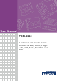
User Manual PCM-9362 3.
Copyright The documentation and the software included with this product are copyrighted 2009 by Advantech Co., Ltd. All rights are reserved. Advantech Co., Ltd. reserves the right to make improvements in the products described in this manual at any time without notice. No part of this manual may be reproduced, copied, translated or transmitted in any form or by any means without the prior written permission of Advantech Co., Ltd. Information provided in this manual is intended to be accurate and reliable.
Product Warranty (2 years) Advantech warrants to you, the original purchaser, that each of its products will be free from defects in materials and workmanship for two years from the date of purchase. This warranty does not apply to any products which have been repaired or altered by persons other than repair personnel authorized by Advantech, or which have been subject to misuse, abuse, accident or improper installation.
Packing List Before installation, please ensure the following items have been shipped: Item Part Number 1 PCM-9362 SBC 1 Startup manual 1 Utility CD 1 mini jumper pack Cables Part Number Description 1700006291 SATA cable 30cm 1703060191 Keyboard/mouse cable 1*6P-2.0/M-DIN 6P(F)*2 19cm 1700000265 WIRE ATX-20P(M)/12P(F) 10CM 1703100152 Audio Cable 10P 2.0mm 15cm 1701140201 COM2 cable 14PIN 2.0mm Secondary Port 9PIN(M)20cm 1703100121 USB 2 PORT cable 10P 12cm IDC 2.
Contents Chapter Chapter 1 General Introduction ...........................1 1.1 1.2 1.3 1.4 Introduction ............................................................................................... 2 Product Feature ........................................................................................ 2 Specifications ............................................................................................ 3 1.3.1 Functional Specification ......................................................
3.4 3.5 3.6 3.7 3.8 Chapter Figure 3.10Advanced ACPI Configuration.................................. 29 Figure 3.11Chipset ACPI Configuration ..................................... 30 3.3.6 AHCI Configuration..................................................................... 31 Figure 3.12AHCI Configuration .................................................. 31 3.3.7 APM Configuration...................................................................... 32 Figure 3.13APM Configuration ..................
Table A.7: CN7: COM3/COM4................................................... 65 Table A.8: CN8: AT/ATX Power Input........................................ 66 Table A.9: CN9: MIO 2.0............................................................ 67 Table A.10:CN10: PS2................................................................ 71 Table A.11:CN11: SMBus........................................................... 71 Table A.12:CN17: COM2 ............................................................ 72 Table A.
PCM-9362 User Manual viii
Chapter 1 1 General Introduction This chapter gives background information on the PCM-9362.
1.1 Introduction PCM-9362 is a 3.5" SBC (Single Board Computer) with Embedded Intel® Atom N450/D510 1.67 GHz Processor. The PCM-9362 can support DDR2 memory up to 2GB, has six USB 2.0 compatible ports, two Giga-LAN (1000Mbps) interface, LVDS and VGA support, HD (High Definition) Audio, and one Mini-PCIe expansion. In addition, PCM-9362 also supports two SATA, four COM ports and one CF slot. 1.2 Product Feature General CPU: Intel® Atom™ processor N450/D510 1.
1.3.1 Functional Specification Processor Processor Intel® Atom™ Processor N450/D510 Intel® Atom™ N450/D510 at 1.67 GHz with 512 KB/1MB L2 cache Manufacturing Technology:45nm Memory Intel® N450/D510 Supports DDR2 667 MHz up to 2 GB (does NOT support DDR2 533MHz Memory) SODIMM Socket: 1. 200-pin SODIMM socket type *1 Graphic and Video Controllers Intel 3.5 Gen Integrated Graphic Engine + GFX core * DVMT 3.0 (Dynamic Video Memory Technology) * Directx* 9 compliant Pixel Shader 2.
Other Chipset Graphic and Video Controllers Intel 3.5 Gen Integrated Graphic Engine + GFX core CRT: Intel Atom N450 up to 1400 x 1050 (SXGA) Intel Atom D510 up to 2048 x 1536 LVDS: Single channel 18-bit LVDS up to WXGA 1366 x 768 LVDS connector : Hirose DF13 type 20 pin CRT connector : D-SUB15 at coastline LAN LAN1 Intel 82567, LAN2 Intel 82583V Compliant with IEEE 802.3, IEEE 802.3u, IEEE 802.3x, IEEE 8023y, IEEE 802.ab. Support 1000Mbps.
Chapter 1 1.3.3 Electrical Specification 1.3.3.1 Power supply Voltage Voltage requirement with AT/ATX Power: AT: +5 VDC ±5% or +12 VDC ±5% or +5 VDC ±5%, +5 V Standby for ATX mode (12 V is optional for LCD inverter and add on card) 1.3.3.2 Power Supply Current Supply Current (ATX) - Typical in XP mode: PCM-9362NC-S6A1E: 5 V : 2.31 A PCM-9362N-S6A1E: 12 V : 0.87 A PCM-9362D-S6A1E: 12 V : 0.91 A - Max in HCT: PCM-9362NC-S6A1E: 5 V : 2.36 A PCM-9362N-S6A1E: 12 V : 1.01 A PCM-9362D-S6A1E: 12 V : 1.17 A 1.3.3.
PCM-9362 User Manual 6
Chapter 2 2 H/W installation This chapter explains the setup procedures of the PCM-9362 hardware, including instructions on setting jumpers and connecting peripherals, switches, indicators and mechanical drawings. Be sure to read all safety precautions before you begin the installation procedure.
2.1 Jumpers 2.1.1 Jumper list Table 2.1: Jumper List J2 COM2 Setting J3 AT / ATX Power SEL J4 Clear CMOS J5 Panel Voltage SEL 2.1.2 Jumper Settings Table 2.2: J2: COM2 Setting Part Number 1653003260 Footprint HD_3x2P_79 Description PIN HEADER 3*2P 180D(M) 2.0mm SMD SOUARE PIN Setting Function (1-2) RS232 (3-4) RS485 (5-6) RS422 Table 2.3: J3: AT / ATX Power SEL Part Number 1653002101 Footprint HD_2x1P_79_D Description PIN HEADER 2*1P 180D(M)SQUARE 2.
Part Number 1653003101 Footprint HD_3x1P_79_D Description PIN HEADER 3*1P 180D(M) 2.0mm DIP SQUARE W/O Pb Setting Function (1-2) Normal (2-3) Clear CMOS Chapter 2 Table 2.4: J4: Clear COMS H/W installation Table 2.5: J5: PAN VOL SEL Part Number 1653003101 Footprint HD_3x1P_79_D Description PIN HEADER 3*1P 180D(M) 2.
2.1.3 Jumper Description Cards can be configured by setting jumpers. A jumper is a metal bridge used to close an electric circuit. It consists of two metal pins and a small metal clip (often protected by a plastic cover) that slides over the pins to connect them. To close a jumper, you connect the pins with the clip. To open a jumper, you remove the clip. Sometimes a jumper will have three pins, labeled 1, 2 and 3. In this case you would connect either pins 1 and 2, or 2 and 3.
Chapter 2 2.2 Connectors 2.2.1 Connector list Table 2.6: Connector list Audio CN2 SATA CN3 SATA CN4 GPIO CN5 HDD & PWR LED CN6 12V AT Power Input CN7 COM3/COM4 CN8 AT/ATX Power Input CN9 MIO 2.
2.2.2 Connector Settings 2.2.2.1 Audio Interface (CN1) Audio Port Connectors One 5 x 2 pin box header for Audio connector. These audio connectors are used for audio devices. The audio jacks are differentiated by color for different audio sound effects. 2.2.2.2 SATA Connector (CN2, CN3) PCM-9362 supports Serial ATA via two connectors (CN2, CN3). Data transfer rates up to 300 MB/s are possible, enabling very fast data and file transfer, and independent DMA operation on two ports. 2.2.2.
2.2.2.10 Inverter Power Connector (CN13) PCM-9362 can provide +5 V and +12 V and signal to LCD inverter board via CN13. 2.2.2.11 USB Connectors (CN14, CN15, CN24, CN25) The board provides up to six USB (Universal Serial Bus) ports. This gives complete Plug and Play, and hot attach/detach for up to 127 external devices. The USB interfaces comply with USB specification Rev. 2.0 which supports 480 Mbps transfer rate, and are fuse protected.
2.2.2.14 Power Switch Connector (CN20) One 2 x 1 pin wafer box (CN20) for power switch. 2.2.2.15 LPT Connector (CN21) PCM-9362 can support LPT via CN21. LPT (Line Print Terminal) is the original, yet still common, name of the parallel port interface on IBM PC-compatible computers. It was designed to operate a text printer that used IBM's 8-bit extended ASCII character set. 2.2.2.16 Standby Power Connector (CN22) PCM-9362 can support both ATX and AT power supply. 2.2.2.
Chapter 2 2.3 Mechanical 2.3.1 Jumper and Connector Location H/W installation Figure 2.1 Jumper and Connector layout (Component side) Figure 2.
2.3.2 Board Dimension Figure 2.
Chapter 2 H/W installation Figure 2.4 Board Dimension layout (Solder side) Figure 2.
PCM-9362 User Manual 18
Chapter 3 BIOS settings 3
AMIBIOS has been integrated into many motherboards for over a decade. With the AMIBIOS Setup program, you can modify BIOS settings and control the various system features. This chapter describes the basic navigation of the PCM-9362 BIOS setup screens. Figure 3.1 Setup program initial screen AMI's BIOS ROM has a built-in setup program that allows users to modify the basic system configuration. This information is stored in battery-backed CMOS so it retains the setup information when the power is turned off.
When you first enter the BIOS Setup Utility, you will enter the Main setup screen. You can always return to the Main setup screen by selecting the Main tab. There are two Main Setup options. They are described in this section. The Main BIOS Setup screen is shown below. Chapter 3 3.2 Main Setup BIOS settings Figure 3.2 Main setup screen The Main BIOS setup screen has two main frames. The left frame displays all the options that can be configured.
3.3 Advanced BIOS Features Setup Select the Advanced tab from the PCM-9362 setup screen to enter the Advanced BIOS Setup screen. You can select any of the items in the left frame of the screen, such as CPU Configuration, to go to the sub menu for that item. You can display an Advanced BIOS Setup option by highlighting it using the keys. All Advanced BIOS Setup options are described in this section. The Advanced BIOS Setup screens are shown below. The sub menus are described on the following pages.
Chapter 3 3.3.1 CPU Configuration BIOS settings Figure 3.4 CPU Configuration Setting Max CPUID Value Limit This item allows you to limit CPUID maximum value. Execute-Disable Bit Capability This item allows you to enable or disable the No-Execution page protection technology. Hyper Threading Technology This item allows you to enable or disable Intel® Hyper Threading technology.
3.3.2 IDE Configuration Figure 3.5 IDE Configuration ATA/IDE Configuration This item allows you to select Disabled / Compatible / Enhanced. Legacy IDE Channels When set to Enhanced mode you can select IDE or AHCI mode. When select Compatible mode you can select SATA only / SATA pri, PATA sec or PATA only. Primary/Secondary/Third IDE Master/Slave BIOS auto detects the presence of IDE device, and displays the status of auto detection of IDE device. >Type: Select the type of SATA driver.
Chapter 3 3.3.3 Super I/O Configuration BIOS settings Figure 3.6 Super I/O Configuration Serial Port1 / Port2 / Port3 / Port 4 address This item allows you to select serial port1 ~ port4 of base addresses. Serial Port1 / Port2 / Port3 / Port 4 IRQ This item allows you to select serial port1 ~ port4 of IRQ. RS-485 Control for SP2 This item allows you to select RS485 control. Auto Direction Control Select This item allows you to enable or disable auto flow control function.
3.3.4 Hardware Health Configuration Figure 3.7 Hardware health configuration H/W Health Function This item allows you to control H/W monitoring. Temperature & Voltage show CPU/System Temperature Vcore / +3.
Chapter 3 3.3.5 ACPI Settings BIOS settings Figure 3.
3.3.5.1 General ACPI Configuration Figure 3.9 General ACPI Configuration Suspend mode Select the ACPI state used for system suspend. Report Video on S3 Resume This item allows you to invoke VA BIOS POST on S3/STR resume.
Chapter 3 3.3.5.2 Advanced ACPI Configuration BIOS settings Figure 3.10 Advanced ACPI Configuration ACPI Version Features This item allows you to enable RSDP pointers to 64-bit fixed system description tables. ACPI APIC support Include APIC table pointer to RSDT pointer list. AMI OEMB table Include OEMB table pointer to R(x)SDT pointer lists. Headless mode Enable / Disable Headless operation mode through ACPI.
3.3.5.3 Chipset ACPI Configuration Figure 3.11 Chipset ACPI Configuration Energy Lake Feature Allows you to configure Intel's Energy Lake power management technology. APIC ACPI SCI IRQ Enable/Disable APIC ACPI SCI IRQ. USB Device Wakeup From S3/S4 Enable/Disable USB Device Wakeup from S3/S4. High Performance Event Timer Enable/Disable High performance Event timer.
Chapter 3 3.3.6 AHCI Configuration BIOS settings Figure 3.12 AHCI Configuration AHCI Port0 / Port1 While entering setup, BIOS auto detects the presence of IDE devices. This displays the status of auto detection of IDE device.
3.3.7 APM Configuration Figure 3.13 APM Configuration Power Management/APM Enable or disable APM. Power Button Mode Power on, off, or enter suspend mode when the power button is pressed. The following options are also available. Restore on AC power Loss Use this to set up the system response after a power failure.
Chapter 3 3.3.8 Event Log Configuration BIOS settings Figure 3.14 Event Log Configuration View Event Log View all unread events on the event Log. Mark all events as read Mark all unread events as read. Clear Event Log Discard all events in the event Log.
3.3.9 MPS Configuration Figure 3.15 MPS Configuration MPS Revision This item allows you to select MPS reversion.
Chapter 3 3.3.10 Smbios Configuration BIOS settings Figure 3.16 Smbios Configuration Smbios Smi Support SMBIOS SMI wrapper support for PnP function 50h-54h.
3.3.11 USB Configuration Figure 3.17 USB Configuration Legacy USB Support Enables support for legacy USB. Auto option disables legacy support if no USB devices are connected. USB 2.0 Controller Mode This item allows you to select HiSpeed(480Mbps) or FullSpeed (12Mpbs). BIOS EHCI Hand-Off This is a workaround for OS without EHCI hand-off support. The EHCI ownership change should claim by EHCI driver. Hotplug USB FDD Support A dummy FDD device is created that will be associated with the hotplugged FDD later.
Chapter 3 >>> USB Mass Storage Device Configuration BIOS settings Figure 3.18 USB Mass storage Device Configuration USB Mass Storage Reset Delay Number of sends POST wait for the USB mass storage device after start unit command. Emulation Type If Auto, USB devices less than 530MB will be emulated as a floppy drive and the remaining as hard drive. Force FDD option can be used to force a FDD formatted drive to boot as FDD (Ex. ZIP drive).
3.4 Advanced PCI/PnP Settings Select the PCI/PnP tab from the PCM-9362 setup screen to enter the Plug and Play BIOS Setup screen. You can display a Plug and Play BIOS Setup option by highlighting it using the keys. All Plug and Play BIOS Setup options are described in this section. The Plug and Play BIOS Setup screen is shown below. Figure 3.19 PCI/PNP Setup (top) Clear NVRAM Set this value to force the BIOS to clear the Non-Volatile Random Access Memory (NVRAM).
Figure 3.20 Boot Setup Utility 39 PCM-9362 User Manual BIOS settings 3.5 Boot Settings Chapter 3 OffBoard PCI/ISA IDE Card Some PCI IDE cards may require this to be set to the PCI slot number that is holding the card. When set to Auto will works for most PCI IDE cards. IRQ3 / 4 / 5 / 7 / 9 / 10 /11 This item allows you respectively assign an interruptive type for IRQ-3, 4, 5, 7, 9, 10, 11.
3.5.1 Boot settings Configuration Figure 3.21 Boot Setting Configuration Quick Boot This item allows BIOS to skip certain tests while booting. This will decrease the time needed to boot the system. Quiet Boot If this option is set to Disabled, the BIOS displays normal POST messages. If Enabled, an OEM Logo is shown instead of POST messages. AddOn ROM Display Mode Set display mode for option ROM. Bootup Num-Lock Select the Power-on state for Numlock. PS/2 Mouse Support Select support for PS/2 Mouse.
Chapter 3 3.6 Security Setup BIOS settings Figure 3.22 Password Configuration Select Security Setup from the PCM-9362 Setup main BIOS setup menu. All Security Setup options, such as password protection and virus protection are described in this section. To access the sub menu for the following items, select the item and press : Change Supervisor / User Password Boot Sector Virus protection: The boot sector virus protection will warn if any program tries to write to the boot sector.
3.7 Advanced Chipset Settings Figure 3.
Chapter 3 3.7.1 North Bridge Chipset Configuration BIOS settings Figure 3.24 North Bridge Configuration DRAM Frequency This item allows you to manually change DRAM frequency. Configure DRAM Timing by SPD This item allows you to enables or disable detection by DRAM SPD. Memory Hole This item allows you to free 15MB-16MB of memory size for some ISA devices. Initate Graphic Aadapter This item allows you to select which graphics controller to use as the primary boot device.
Figure 3.25 Video function configuration DVMT Mode Select Displays the active system memory mode. DVMT/FIXED Memory Specify the amount of DVMT / FIXED system memory to allocate for video memory. Boot Display Device Select boot display device at post stage. Flat Panel Type This item allows you to select which panel resolution you want. Spread Spectrum Clock This item allows you to enable or disable the spread spectrum clock.
Chapter 3 3.7.2 South Bridge Chipset Configuration BIOS settings Figure 3.26 South Bridge Configuration USB Functions Disabled, 2 USB Ports, 4 USB Ports, 6 USB Ports or 8 USB Ports. USB 2.0 Controller Enables or disables the USB 2.0 controller. Internal LAN controller Enables or disables the internal LAN controller. Internal LAN Bootroom Enables or disables internal LAN boot. GbE controller Enables or disables the GbE controller. GbE LAN Boot Enables or disables GbE LAN boot.
3.8 Exit Option Figure 3.27 Exit Option 3.8.1 Save Changes and Exit When you have completed system configuration, select this option to save your changes, exit BIOS setup and reboot the computer so the new system configuration parameters can take effect. 1. Select Exit Saving Changes from the Exit menu and press . The following message appears: Save Configuration Changes and Exit Now? [Ok] [Cancel] 2. Select Ok or cancel. 3.8.
The PCM-9362 automatically configures all setup items to optimal settings when you select this option. Optimal defaults are designed for maximum system performance, but may not work best for all computer applications. In particular, do not use the Optimal Defaults if your computer is experiencing system configuration problems. Select Load Optimal Defaults from the Exit menu and press . 3.8.
PCM-9362 User Manual 48
Chapter 4 4 S/W Introduction & Installation
4.1 S/W Introduction The mission of Advantech Embedded Software Services is to "Enhance quality of life with Advantech platforms and Microsoft Windows embedded technology.” We enable Windows embedded software products on Advantech platforms to more effectively support the embedded computing community. Customers are freed from the hassle of dealing with multiple vendors (Hardware suppliers, System integrators, Embedded OS distributor) for projects.
4.3.2.1 The GPIO API General Purpose Input/Output is a flexible parallel interface that allows a variety of custom connections. It allows users to monitor the level of signal input or set the output status to switch on/off a device. Our API also provides Programmable GPIO, which allows developers to dynamically set the GPIO input or output status. 4.3.2.
4.3.2.5 The Watchdog API A watchdog timer (abbreviated as WDT) is a hardware device which triggers an action, e.g. rebooting the system, if the system does not reset the timer within a specific period of time. The WDT API in SUSI provides developers with functions such as starting the timer, resetting the timer, and setting the timeout value if the hardware requires customized timeout values. 4.3.2.
4.3.4 SUSI Installation 4.3.4.1 Windows XP In windows XP, you can install the library, drivers and demo programs onto the platform easily using the installation tool--The SUSI Library Installer. After the installer has executed, the SUSI Library and related files for Windows XP can be found in the target installation directory. The files are listed in the following table. Directory Contents \Library Susi.lib Library for developing the applications on Windows XP. Susi.
4.3.4.2 Windows CE In windows CE, there are three ways to install the SUSI Library, you can install it manually or use Advantech CE-Builder to install the library or just copy the programs and the library onto a compact flash card. Express Installation: You can use Advantech CE-Builder to load the library into the image. First, you click the My Component tab. In this tab, you click Add New Category button to add a new category, eg. the SUSI Library.
Chapter 4 SusiDemo.exe The SusiDemo.exe test application is an application which uses all functions of the SUSI Library. It has five major function blocks: Watchdog, GPIO, SMBus, I2C and VGA control. The following screen shot appears when you execute SusiDemo.exe. You can click function tabs to select test functions respectively. Some function tabs will not show on the test application if your platform does not support such functions. For a complete support list, please refer to Appendix A.
– Click the READ GPIO DATA button and the status of the GPIO pin will be displayed in (R/W) Result field. Test Read Multiple Input Pin – Click the radio button- Multiple-Pins. – Key in the pin number from ‘0x01’ to ‘0x0F’ to read the value of the input pin. The pin numbers are ordered bitwise, i.e. bit 0 stands for GPIO 0, bit 1 stands for GPIO 1, etc. For example, if you want to read pin 0, 1, and 3, the pin numbers should be ‘0x0B’.
Write a byte – Click the radio button- Access a byte. – Key in the slave device address in Slave address field. – Key in the register offset in Register Offset field. – Key the desired data in the Result field to write to the device. – Click the WRITE SMBus DATA button and then the data will be written to the device through SMBus. Read a word – Click the radio button- Access a word. – Key in the slave device address in the Slave address field.
Write a word – Click the radio button- Access a word. – Key in the slave device address in the Slave address field. – Key in the register offset in the Register Offset field. – Key in the desired data, such as 0x1234, in the Result field to write to the device. – Click the WRITE SMBus DATA button and the data will be written to the device through the SMBus. Read Multiple bytes – Click the radio button- Access multiple bytes. – Key in the slave device address in the Slave address field.
Watchdog When the application is executed, it will display watchdog information in the WATCHDOG INFORMATION group box. It displays max timeout, min timeout, and timeout steps in milliseconds. For example, a 1~255 seconds watchdog will has 255000 max timeout, 1000 min timeout, and 1000 timeout steps. You can test the functionality of the watchdog as follows: Set the timeout value 3000 (3 sec.) in the SET TIMEOUT field and set the delay value 2000 (2 sec.
Hardware Monitor When the Monitor application is executed by clicking the button, hardware monitoring data values will be displayed. If certain data values are not supported by the platform, the correspondent data field will be grayed-out with a value of 0. For More detail PCM-9362 software API user manual, please contact your dealer or Advantech AE. We also include these manuals in this CD.
Appendix A A PIN Assignments
A.1 PIN Assignments Table A.1: CN1: Audio Part Number 1653205260 Footprint HD_5x2P_79_BOX Description BOX HEADER SMD 5*2 180D (M) 2.0mm Pin Pin Name 1 LOUTR 2 LINR 3 GND 4 GND 5 LOUTL 6 LINL 7 GND 8 GND 9 MIC1R 10 MIC1L Matching Cable : 1703100152 Table A.2: CN2: SATA Part Number 1654002320 Footprint FOX_LD1107V-S33T5 Description Serial ATA 7P 1.
Part Number 1654002320 Footprint FOX_LD1107V-S33T5 Description Serial ATA 7P 1.27 90D(M) SMD LD1107V-S33T5 Pin Pin Name 1 GND 2 TX+ 3 TX- 4 GND 5 RX- 6 RX+ 7 GND Table A.4: CN4: GPIO Part Number 1653005261 Footprint HD_5x2P_79 Description PIN HEADER SMD 5*2P 180D(M) 2.0mm Pin Pin Name 1 +5V 2 GPIO4 3 GPIO0 4 GPIO5 5 GPIO1 6 GPIO6 7 GPIO2 8 GPIO7 9 GPIO3 10 GND 63 PCM-9362 User Manual Appendix A PIN Assignments Table A.
Table A.5: CN5: HDD & PWR LED Part Number 1655306020 Footprint WHL6V-2M Description WAFER BOX 2.0mm 6P 180D(M) W/LOCK Pin Pin Name 1 +5V 2 GND 3 Power LED+ 4 Power LED- 5 HDD LED+ 6 HDD LED- Table A.6: CN6: 12V AT Power Input Part Number 1655404090 Footprint ATXCON-2X2-42 Description ATX PWR CONN. 2*2P 180D 4.
Part Number 1653210260 Footprint HD_10x2P_79_BOX Description BOX HEADER 10*2P 180D(M) 2.0mm SMD W/O Pb Pin Pin Name 1 DCD3# 2 DSR3# 3 RXD3 4 RTS3# 5 TXD3 6 CTS3# 7 DTR3# 8 RI3# 9 GND 10 GND 11 DCD4# 12 DSR4# 13 RXD4 14 RTS4# 15 TXD4 16 CTS4# 17 DTR4# 18 RI4# 19 GND 20 GND 65 PCM-9362 User Manual Appendix A PIN Assignments Table A.
Table A.8: CN8: AT/ATX Power Input Part Number 1655412090 Footprint ATXCON-2X6V-42 Description Power CONN.
Part Number 1654000073 Footprint QSE-D160P Description B/B CONN. 80*2P 180D SMD 0.
Table A.9: CN9: MIO 2.
Appendix A PIN Assignments Table A.9: CN9: MIO 2.
Table A.9: CN9: MIO 2.
Part Number 1655306020 Footprint WHL6V-2M Description WAFER BOX 2.0mm 6P 180D(M) W/LOCK Pin Pin Name 1 KBCLK 2 KBDAT 3 MSCLK 4 GND 5 +5V 6 MSDAT Matching Cable: 1703060053 1700060202 Table A.11: CN11: SMBus Part Number 1655904020 Footprint FPC4V-125M Description Wafer SMT 1.25mmS/T type 4P 180D(M) 85205-04001 Pin Pin Name 1 GND 2 SMB_DAT 3 SMB_CLK 4 +5V 71 PCM-9362 User Manual Appendix A PIN Assignments Table A.
Table A.12: CN17: COM2 Part Number 1653207260 Footprint HD_7x2P_79_BOX Description BOX HEADER SMD 7*2P 180D(M) 2.0mm Pin Pin Name 1 DCD# 2 DSR# 3 RXD 4 RTS# 5 TXD 6 CTS# 7 DTR# 8 RI# 9 GND 10 GND 11 422/485TX+ 12 422/485TX- 13 422RX+ 14 422RX- Matching Cable : 1701140201 Table A.13: CN13: Inverter Power Output Part Number 1655000453 Footprint WHL5V-2M-24W1140 Description WAFER BOX 2.
Part Number 1653005260 Footprint HD_5x2P_79_N10 Description PIN HEADER 2*5P 180D(M) 2.0mm SMD IDIOT-PROOF Pin Pin Name 1 +5V 2 +5V 3 A_D- 4 B_D- 5 A_D+ 6 B_D+ 7 GND 8 GND 9 GND Matching Cable : 1703100121 Table A.15: CN15: Internal USB Part Number 1653005260 Footprint HD_5x2P_79_N10 Description PIN HEADER 2*5P 180D(M) 2.
Table A.16: CN16: 18 bits LVDS Panel Part Number 1653910261 Footprint SPH10X2 Description *CONN. SMD 10*2P 180D(M)DF13-20DP-1.25V(91) HRS Pin Pin Name 1 GND 2 GND 3 LVDS0_D0+ 4 NC 5 LVDS0_D0- 6 NC 7 LVDS0_D1+ 8 NC 9 LVDS0_D1- 10 NC 11 LVDS0_D2+ 12 NC 13 LVDS0_D2- 14 NC 15 LVDS0_CLK+ 16 NC 17 LVDS0_CLK- 18 NC 19 +5V or +3.3V 20 +5V or +3.
Part Number 1652000174 Footprint RJ45_28P_RTB-19GB9J1A Description PHONE JACK RJ45 28P DIP Gold flash RTB-19GB9J1A Pin Pin Name 1 TX+(10/100),BI_DA+(GHz) 2 TX-(10/100),BI_DA-(GHz) 3 RX+(10/100),BI_DB+(GHz) 4 BI_DC+(GHz) 5 BI_DC-(GHz) 6 RX-(10/100),BI_DB-(GHz) 7 BI_DD+(GHz) 8 BI_DD-(GHz) Table A.
Table A.19: CN19: LAN2 Part Number 1652002996 Footprint RJ45_14P_RTA-195AAK1A Description Phone Jack RJ45 14P 90D(M) DIP RTA-195AAK1A Pin Pin Name Table A.20: CN20: Power Switch (Low Active ) Part Number 1655302020 Footprint WF_2P_79_BOX_R1_D Description WAFER BOX 2P 180D(M) 2.0mm W/Lock Pin Pin Name 1 PSIN 2 GND Table A.21: CN11: LPT Part Number 1653213260 Footprint HD_13x2P_79_BOX Description BOX HEADER 13*2P 180D(M) 2.
Appendix A PIN Assignments Table A.21: CN11: LPT 13 D5 14 GND 15 D6 16 GND 17 D7 18 GND 19 ACK# 20 GND 21 BUSY 22 GND 23 PE 24 GND 25 SLCT 26 NC Matching Cable : 1700260250 1700001531 Table A.22: CN22: Standby Power Input Part Number 1655303020 Footprint WHL3V-2M Description WAFER BOX 2.
Table A.23: CN2: Reset Part Number 1655302020 Footprint WF_2P_79_BOX_R1_D Description WAFER BOX 2P 180D(M) 2.0mm W/Lock Pin Pin Name 1 RESET# 2 GND Table A.24: CN24: External USB Part Number 1654904105 Footprint USB-V-4A Description USB CON.
Appendix A PIN Assignments Table A.25: CN25: External USB Part Number 1654904105 Footprint USB-V-4A Description USB CON. 4P 90D(F) DIP A TYPE RoHS Pin Pin Name 1 +5V 2 D- 3 D+ 4 GND Table A.26: CN26: COM1 Part Number 1654000056 Footprint DBCOM-VM5MS Description D-SUB CON.
Table A.27: CN27: VGA Part Number 1654000055 Footprint DBVGA-VF5MS Description D-SUB Conn.
Part Number 1654002539 Footprint FOX_AS0B226-S68K7F_HOLDER Description MINI PCI Express LATCH 52P 90D SMD 6.8mm Pin Pin Name 81 PCM-9362 User Manual Appendix A PIN Assignments Table A.
Table A.29: CN29: Mini PCIE slot Part Number 1654002538 Footprint FOX_AS0B226-S68K7F Description MINI PCI express 52P 90D SMD H=6.8mm Pin Pin Name 1 WAKE# 2 +3.3V or +3.3VSB 3 NC 4 GND 5 NC 6 +1.5V 7 CLKREQ# 8 NC 9 GND 10 NC 11 REFCLK- 12 NC 13 REFCLK+ 14 NC 15 GND 16 NC 17 NC 18 GND 19 NC 20 NC 21 GND 22 PERST# 23 PERn0 24 +3.3VSB 25 PERp0 26 GND 27 GND 28 +1.
Appendix A PIN Assignments Table A.29: CN29: Mini PCIE slot 43 GND 44 NC 45 NC 46 NC 47 NC 48 +1.5V 49 NC 50 GND 51 NC 52 +3.3V or +3.
Table A.30: CN30: DDR2 SODIMM Part Number 1651000087 Footprint DDR-SODIMM-STD65 Description SKT DIMM 200P DDR2 H=6.
Appendix A PIN Assignments Table A.30: CN30: DDR2 SODIMM 43 DQ47 44 DQ43 45 DQ46 46 DQ42 47 GND 48 GND 49 DQS#5 50 NC 51 DQS5 52 DM5 53 GND 54 GND 55 DQ45 56 DQ41 57 DQ44 58 DQ40 59 GND 60 GND 61 DQ39 62 DQ35 63 DQ38 64 DQ34 65 GND 66 GND 67 DM4 68 DQS#4 69 NC 70 DQS4 71 GND 72 GND 73 DQ37 74 DQ33 75 DQ36 76 DQ32 77 GND 78 GND 79 CKE0 80 CKE1 81 +1.8V 82 +1.8V 83 NC 84 NC 85 BA2 86 A14 87 +1.8V 88 +1.
Table A.30: CN30: DDR2 SODIMM 90 A11 91 A9 92 A7 93 A8 94 A6 95 +1.8V 96 +1.8V 97 A5 98 A4 99 A3 100 A2 101 A1 102 A0 103 +1.8V 104 +1.8V 105 A10 106 BA1 107 BA0 108 RAS# 109 WE# 110 SCS#0 111 +1.8V 112 +1.8V 113 CAS# 114 ODT0 115 SCS#1 116 A13 117 +1.8V 118 +1.
Appendix A PIN Assignments Table A.
Table A.30: CN30: DDR2 SODIMM 184 GND 185 DM0 186 DQS#0 187 GND 188 DQS0 189 DQ5 190 GND 191 DQ4 192 DQ1 193 GND 194 DQ0 195 SDA 196 GND 197 SCL 198 SA0 199 +3.
Part Number 1651000682 Footprint SOCKET_8P_ACA-SPI-004-K01 Description IC SKT 8P SMD WO/Pb C ACA-SPI-004-K01 Pin Pin Name 1 CE# 2 SO 3 WP# 4 GND 5 SI 6 SCK 7 HOLD# 8 +3.3V Table A.32: CN32: CF Part Number 1653002919 Footprint CF_50P_CFCMD-35T15W100 Description CF Type2 Conn.
Table A.
Appendix A PIN Assignments PCM-9362 User Manual 91
www.advantech.com Please verify specifications before quoting. This guide is intended for reference purposes only. All product specifications are subject to change without notice. No part of this publication may be reproduced in any form or by any means, electronic, photocopying, recording or otherwise, without prior written permission of the publisher. All brand and product names are trademarks or registered trademarks of their respective companies. © Advantech Co., Ltd.