
User's Manual


4
www.lairdtech.com
Laird Technologies
LT2510
Wireless Module
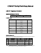
TABLE 2: PIN DEFINITIONS FOR THE LT2510 TRANSCEIVER
SMT PIN PLUGGABLE
PIN
TYPE SIGNAL NAME FUNCTIONS
1 7 O GO_0/
Hop_Frame
Generic Output/Hop_Frame
2 6 O GO_1 Generic Output
3 8 DNC Do not connect.
4 17 Reserved Reserved for future use
5 19 O PWM_Output PWM Output
6 3 I RXD Asynchronous serial data input to transceiver
7 2 O TXD Asynchronous serial data output from transceiver
8 10 GND GND Signal Ground
9 1 PWR Vcc 3.3 - 3.6 V ±50mV ripple (must be connected)
10 - PWR Vpa 3.3 – 3.6 V +/-50mV ripple (must be connected)
11 - GND GND Signal Ground
12 9 I Test Test Mode – When pulled logic Low and then applying power or resetting,
the transceiver’s serial interface is forced to a 9600, 8-N-1 rate. To exit Test
Mode, the transceiver must be reset or power-cycled with Test Mode pulled
logic High or left oating/disconnected.
Note: Because this mode disables some modes of operation, it should not be
permanently pulled Low during normal operation.
13 14 I DI0 Digital Input 0
14 5 I UP_Reset RESET – Controlled by the LT2510 for power-on reset if left
unconnected. After a stable power-on reset, a logic Low pulse will reset the
transceiver.
15 11 I CMD/Data When logic Low, the transceiver interprets OEM Host data as command
data. When logic High, the transceiver interprets OEM Host data as trans-
mit data.
16 15 O In Range When logic low, the client is in range and synchronized with a server. This
will always be low on a Server.
17 16 I RTS Request to Send. Floats high if left unconnected, when enabled the
module
will not transmit data out the Serial UART unless the pin is low
18 12 O CTS Clear to Send - Active Low when the transceiver is ready to accept data for
transmission.
19 14 I DI1 Digital Input 1
20 13 Reserved Reserved for future use. Do not connect.
21 4 Reserved Reserved for future use. Do not connect.
22 20 I AD_In Analog to Digital Input
SPECIFICATIONS
ENGINEER’S TIP
• All I/O is 3.3V TTL.
• All inputs are weakly pulled High via a 20kOhm pull-up resistor and may be left oating during normal operation
• Minimum Connections: VCC, VPA, GND, TXD, & RXD
• Signal direction is with respect to the transceiver
• Unused pins should be left disconnected