
User's Manual


14.7456 MHz VCTCXO
An external clock signal from VCTCXO X1 is connect to CC1020 XOSC_Q1 , This VCTCXO is only
5x3.2x1.4(H) mm, and is manufactured with a ceramic base and metal lid to assure very good aging
characteristics and reliability. This device offers an in ±2.5PPM over -30 to +75 Celsius. The VR1 is used
to adjust the frequency is as close as possible to the exact required transmit frequency. Ideally it should be
within 100 Hz at room temperature.
PA module
The U2 is a power amplifier IC as the final RF amplifier in the 400MHz to 480MHz band.
Low pass filter
The amplifier RF signal is through the harmonic low pass filter, comprising L63 to L65 and C62-C66 and
then to the antenna connector J1.
Antenna switch
When transmitting, the diode D61 and D60 are forward biased, allowing the RF to pass to the antenna. D60
is shorted to ground which makes L61 look open circuit (1/4 wave tuned stub ). This prevents the TX signal
from passing to the receiver stage.
Microcontroller interface
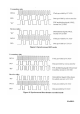
Used in a typical system, CC1020 will interface to a microcontroller. This microcontroller must be able to:
. Program CC1020 into different modes via the 4-wire serial configuration interface (PDI, PDO, PCLK,
and PSEL)
. Interface to the bi-directional synchronous data signal interface (DIO and DCLK)
. Optionally, the microcontroller can do data encoding / decoding
. Optionally, the microcontroller can monitor the LOCK pin for frequency lock status, carrier sense status,
or other status information
. Optionally, the microcontroller can read back digital RSSI value and other status information via 4-wire
serial interface
PAGE6