
User's Manual

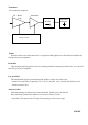


Receiver
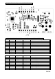
The receiver comprises:
Antenna Switch
In receive, the diode D4 are reverse biased. L212 is now in circuit, passing
the signal from the antenna to the U1 LNA input.
. In the RX path , the voice signal after demodulation is sent to the internal DAC which can directly drive
a 32 ohm resistance loading through AC coupling.
Carrier Detect
A Carrier Detect ( MUTE DETECT ) output is available on pin 6 of JP1 .
When noise is present, the voltage at pin 26 of U1 is LOW. The squelch trigger
output is open, It’s make pin 6 of JP1 open state.
When no noise is
present, the
voltage at pin 26 of U1 is HI voltage.
This make pin 6 of JP1 short state.
Microcontroller
The PIC16F630 microcontroller IC controls the programmable features and frequency synthesizer
Data.
Programming Mode
The programming mode allows the user to retrieve or program TX/RX frequencies,
when pin 9 of J1 is set to ground. Programming mode will Inhibit ,
Serial communications can then be made in order to read/program the on- board
EEPROM ( U3 )which contains radio- specific data.
EEPROM
Relevant channel information, such as Rx/ Tx frequencies, is stored in the EEPROM( U3)
which is built in PIC16F630. This information may be programmed and erased via the test fixture.
The EEPROM has 1024 (8x128) capacity and is written serially.
Power supply circuit
The data radio is supplied with a nominal + 6.0V dc power supply input from external
equipment which is filtered using C56. This supply is converted into 3.3V
voltage levels on the board using the regulator U4 and associated components .
This +3.3V line is fed to the CPU circuit.
PAGE7