
Technical data

1100 Series DAD and MWD Reference Manual 241
Introduction to the Detector 6
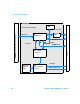
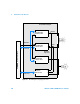
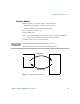
SCI Board
The SCI (spectrograph connector interface), located on the optical unit
assembly is the interface between micro-slit, PDA and detector main board. In
addition, wavelength calibration data and manufacturing data from the
manufacturing process (for example, serial number, dates, and so on) are
stored in the EEPROM.
PDA Signal Conditioning Electronics
Data is transferred from the photodiode array (PDA) through the
spectrograph connector interface (SCI) board to the PDA signal conditioning
electronics. The PDA signal conditioning electronics adjusts the signal levels
to provide an appropriate output signal.
A/D Converter
The output signal from the PDA signal conditioning electronics is directed to
the 16-bit /160-kHz A/D converter. Multiplexing is used to monitor test signals
for diagnostic purposes including GND, reference voltage (Vref), and a ramp
signal. These signals are used to verify the front end electronics separately
from the PDA. The signal from the PDA temperature sensor is used for
temperature compensation.
PFP (PDA Front-end Processor)
The PFP on this board utilizing RAM of 3 × 32 KB and 1 × 8 KB and the EPLD
(electronically programmable logic device) forwards the data from the 16-bit
A/D converter. It provides timing and control for the photodiode readout and
the A/D conversion.
Analog Outputs
There are two independent analog outputs (0…1 V full scale). Digital data from
the ASIC is converted into a pulse-width modulated signal (PWM). The PWM
signal is then fed to an amplitude modulator, which precisely turns the
reference signal on and off. This signal then passes to a low-pass filter section.