SERVICE MANUAL AUTORANGING DC POWER SUPPLY AGILENT MODELS 6010A, 6011A, 6012B and 6015A Agilent Part No. 5964-8275 FOR INSTRUMENTS WITH SERIAL NUMBERS Agilent Model 6010A; Serials US37110171 and above Agilent Model 6011A; Serials US35460156 and above Agilent Model 6012B; Serials US35430336 and above Agilent Model 6015A; Serials US37050146 and above For instruments with higher serial numbers, a change page may be included. Microfiche Part No.
CERTIFICATION Agilent Technologies certifies that this product met its published specifications at time of shipment from the factory. Agilent Technologies further certifies that its calibration measurements are traceable to the United States National Institute of Standards and Technology, to the extent allowed by the Institute’s calibration facility, and to the calibration facilities of other International Standards Organization members.
SAFETY SUMMARY The following general safety precautions must be observed during all phases of operation, service and repair of this instrument. Failure to comply with these precautions or with specific warnings elsewhere in this manual violates safety standards of design, manufacture, and intended use of the instrument. Agilent Technologies, Inc. assumes no liability for the customer's failure to comply with these requirements. BEFORE APPLYING POWER.
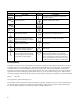
Safety Symbol Definitions Symbol Description Symbol Description Direct current Terminal for Line conductor on permanently installed equipment Alternating current Caution, risk of electric shock Both direct and alternating current Caution, hot surface Three-phase alternating current Caution (refer to accompanying documents) Earth (ground) terminal In position of a bi-stable push control Protective earth (ground) terminal (Intended for connection to external protective conductor.
TABLE OF CONTENTS Introduction ............................................................................................................................................................................ 7 Scope .................................................................................................................................................................................... 7 Calibration and Verification ........................................................................................
DC Power Conversion Subsystem ...................................................................................................................................... 54 Output Subsystem............................................................................................................................................................... 54 The Front Panel Board................................................................................................................................................
1 Introduction Scope This manual contains information for troubleshooting the Agilent Models 6010A, 6011A, 6012B, or 6015A 1000W Autoranging Power Supply to the component level. Wherever applicable, the service instructions given in this manual refer to pertinent information provided in the Operation Manual. Both manuals cover Agilent Models 6010A/11A/12B/15A; differences between models are described as required. The following information is contained in this manual.
Manual Revisions Agilent Technologies instruments are identified by a 10-digit serial number. The format is described as follows: first two letters indicate the country of manufacture. The next four digits are a code that identify either the date of manufacture or of a significant design change. The last four digits are a sequential number assigned to each instrument. Item Description US The first two letters indicates the country of manufacture, where US = USA; MY = Malaysia.
2 Calibration and Verification Introduction This section provides test and calibration procedures. The operation-verification tests comprise a short procedure to verify that the unit is performing properly, without testing all specified parameters. After troubleshooting and repair of a defective power supply you can usually verify proper operation with the turn-on checkout procedure in the Operating Manual.
Table 2-1. Test Equipment Required TYPE Oscilloscope REQUIRED CHARACTERISTICS Sensitivity: 1mV Bandwidth: 20MHz & 100MHz Input: differential, 50Ω & 10MΩ USE P,T Isolation Transformer 100VA 4KVA minimum T RMS Voltmeter True rms, 10MHz bandwidth Sensitivity: 1 mV Accuracy: 5% P Agilent 3400A Logic Pulser 4.5 to 5.5Vdc @ 35mA T Agilent 546A Multimeter Resolution: 100nV Accuracy: 0.
Table 2-1. Test Equipment Required (continued) TYPE Load Resistors (6015A) REQUIRED CHARACTERISTICS 40Ω, ±1%, 1000W 250Ω, ±1%, 1000W USE P,A Current-Monitoring Resistors Value: 6010A P,A RECOMMENDED MODEL 100mV @ 10A (10mΩ must be capable of 20Amps) Accuracy: 0.02% ** TC: 10ppm/°C 6011A 50mV @100A (0.5mΩ) Accuracy: 0.05% ** TC: 30ppm/°C 6012B 50mV @ 50A (1.0mΩ) Accuracy: 0.02% ** TC: 30ppm/°C 6015A 0.1Ω, 15A, ±0.
Initial Setup Maintenance described herein is performed with power supplied to the instrument, and protective covers removed. Such maintenance should be performed only by service trained personnel who are aware of the hazards involved (for example, fire and electrical shock). Turn off ac power when making or removing connections to the power supply. Where maintenance can be performed without power applied, the power should be removed. a. b. c. d. e. f.
Table 2-2. Calibration Procedure (continued) TEST V-MON Zero Adjust. TESTED VARIABLE V-MON TEST POINTS VM ( + ) M(-) TEST SEQUENCE AND ADJUSTMENTS a. b. c. d. Common Mode Adjust. Residual Output Voltage VM( + ) VM ( + ) M(-) a. b. c. d. I-MON Zero Adjust. I-MON IM ( + ) M (-) e. f. a. b. c. I-MON F/S Adjust. I-MON IM ( + ) M(-) a. b. c. d. Rm ( + ) Rm ( - ) e. Set voltage and current controls to minimum settings. Disable power supply as in Initial Setup step i.
Table 2-2. Calibration Procedure (continued) TEST Power Limit Adjust. TESTED VARIABLE V(OUT) I(OUT) TEST POINTS TEST SEQUENCE AND ADJUSTMENTS a. b. Perform I-MON F/S Adjust before proceeding. Connect the unit to the ac power line via a variable transformer. Set input power rail to 240Vdc; DVM ( + ) on rear of A1R3 and DVM (-) to rear of A1R1. Note that power rail must be maintained at 240Vdc during calibration. WARNING The inner cover must be removed to connect the voltmeter.
Table 2-2. Calibration Procedure (continued) TEST Power Limit Adjust (continued) TESTED VARIABLE TEST POINTS TEST SEQUENCE AND ADJUSTMENTS h. Turn A2R26 (upper knee) fully counter clockwise. Turn on the supply and set voltage at 200V (6010A), 20V (6011A), 60V (6012B), 500V (6015A), and current at 5.25A (6010A), 56A (6011A), 19A (6012B) 2.25A (6015A), using DISPLAY SETTINGS. i. Turn A2R26 (upper knee) clockwise until CV LED lights. Output should be 200 ± 2V (6010A), 20 ±0.5V (6011A), 60 ±0.
Table 2-3. Guide to Recalibration After Repair Printed Circuit Board A1 Main Board Block Name Circuit Within A1 Main Board A5 Diode Board A2 Control Board A2 Control Board A2 Control Board A2 Control Board A2 Control Board A2 Control Board 1. 2. 3. Constant Voltage (CV) Circuit Constant Voltage (CV) Circuit Constant Current (CC) Circuit Power Limit Comparator Bias Power Supplies All Except Current Source Current Source Ref.
for the electronic load in the following tests: CV Source Effect (Line Regulation) CC Load Effect (Load Regulation) Temperature Coefficient (6015A) Drift (stability ) (6015A) You may substitute: 40Ω 1000W load resistor (6010A) 0.058Ω 1000W load resistor (6011A) 3.
Constant Voltage (CV) Tests CV Setup. If more than one meter or a meter and an oscilloscope are used, connect each to the + S and - S terminals by a separate pair of leads to avoid mutual coupling effects. Connect only to + S and -S (except for peak-to-peak PARD) because the unit regulates the output voltage between + S and - S, not between + OUT and -OUT. Use coaxial cable or shielded 2-wire cable to avoid pickup on test leads. For all CV tests set the output current at full output to assure CV operation.
g. When the reading settles, record the output voltage again. Check that the two recorded readings differ no more than: ± 0.011Vdc (6010A) ± 0.0037Vdc (6011A) ± 0.007Vdc (6012B) ± 0.033Vdc (6015A) Source Effect (Line Regulation). Source effect is the change in dc output voltage resulting from a change in ac input voltage from the minimum to the maximum value as specified in Input Power Requirements in the Specifications Table, in the Operating Manual. Proceed as follows: a.
d. e. Reduce the resistance of the load to draw an output current of: 17.0Adc (6010A) 120Adc (6011A) 17.5Adc (6012B) 5.0Adc (6015A) Check that the unit's CV LED remains lighted. Check that the rms noise voltage at the true rms voltmeter is no more than: 22mV rms (6010A) 8.0mV rms (6011A) 8.0mV rms (6012B) 50mV rms (6015A) Figure 2-4. RMS Measurement Test Setup, CV PARD Test Peak Measurement Procedure. Figure 2-5 shows the interconnections of equipment to measure PARD in Vpp.
d. e. f. 60Vdc (6012B) 200Vdc (6015A) Reduce the resistance of the load to draw an output current of: 17.0Adc (6010A) 120Adc (6011A) 17.5Adc (6012B) 5.0Adc (6015A) Check that the unit's CV LED remains lighted. Set the oscilloscope's input impedance to 50Ω and bandwidth to 20MHz. Adjust the controls to show the 20KHz and higher frequency output-noise waveform of Figure 2-6. Check that the peak-to-peak is no more than: 50mV (6010A) 50mV (6011A) 50mV (6012B) 160mV (6015A) Figure 2-5.
6010A 6011A NOT APPLICABLE 6012B 6015A Figure 2-6. 20KHz Noise, CV Peak-to-Peak PARD Proceed as follows: a. b. c. d. e. f. 22 Connect the test equipment as shown in Figure 2-3. Operate the load in constant-current mode and set for minimum current. Turn the unit's power-on, and turn up current setting to full output. Turn up output voltage to: 60Vdc (6010A) 7.0Vdc (6011A) 20.0Vdc (6012B) 200Vdc (6015A) as read on the digital voltmeter.
g. Check that the pulse width of the transient pulse is no more than: 150mV/2ms (6010A) 100mV/2ms (6011A) 100mV/2ms (6012B) 200mV/5ms (6015A) 6010A 6011A 6012B 6015A Figure 2-7. Load Transient Recovery Waveform Temperature Coefficient. Temperature coefficient (TC) is the change in output voltage for each °C change in ambient temperature with constant ac line voltage, constant output voltage setting and constant load resistance.
e. f. g. h. 200Vdc (6010A) 20.0Vdc (6011A) 60.0Vdc (6012B) 500Vdc (6015A) as read on the DVM. After 30 minutes stabilization, record the temperature to the nearest 0.1°C. Record the output voltage on the DVM. Set oven temperature to 50°C. After 30 minutes stabilization, record the temperature to the nearest 0.1°C. Record output voltage. Check that the magnitude of the output voltage change is no greater than 620mV.(6010A) 80mV (6011A) 176mV (6012B) 1.6V (6015A) Drift (Stability).
d. e. f. g. h. 17.5Adc (0.0175Vdc across Rm) (6012B) Check that the AMPS display reads about 17.5 amps. 2Adc (0.20Vdc across Rm) (6015A) Check that the AMPS display reads about 2 amps. Increase the load resistance until the output voltage at +S and -S increases to: 200Vdc (6010A) 20Vdc (6011A) 60Vdc (6012B) 500Vdc (6035A) Check that the CC LED is lighted and AMPS display still reads ≈ current setting. Record voltage across Rm. Short circuit the load.
load resistor that is capable of safely dissipating 1000 watts. Proceed as follows: a. Connect the test equipment as shown in Figure 2-8. b. Switch the unit's power-on and turn the output voltage all the way up. c. Turn up output current to: 17.0Adc (6010A) 120Adc (6011A) 50Adc (6012B) 5.0Adc (6015A) Check that the unit's CC LED remains lighted. d. Check that the rms noise current measured by the current probe and rms voltmeter is no more than: 15mA rms (6010A).
3 Troubleshooting Maintenance described herein is performed with power supplied to the instrument, and protective covers removed. Such maintenance should be performed only by service-trained personnel who are aware of the hazards involved (for example, fire and electrical shock). Where maintenance can be performed without power applied, the power should be removed.
Table 3-1. Control Board Test Connector, A2J7 PIN NO. SIGNAL NAME Digital-Circuits Bias & Reference Voltages 24 +5V 22 + 20V(5V UNREG) 14 2.5V ref 6 0.5V ref Analog-Circuits Bias Voltages 2 + 15V 21 - 15V Vdc 5.0 20.0 2.50 0.50 WAVEFORM/CONDITIONS with 120Hz & 40KHz ripple 15.0 -15.
Electrostatic Protection The following caution outlines important precautions which should be observed when working with static sensitive components in the power supply. This instrument uses components which can be damaged by static charge. Most semiconductors can suffer serious performance degradation as a result of static charges, even though complete failure may not occur. The following precautions should be observed when handling static-sensitive devices. a. b. c. d. e. f.
To avoid the possibility of personal injury, remove the power supply from operation before opening the cabinet. Turn off ac power and disconnect the line cord, load, and remote sense leads before attempting any repair or replacement. When replacing any heatsink-mounted components except thermostat, smear a thin coating of heatsink compound between the component and heatsink. If a mica insulator is used, smear a thin coating of heatsink compound on both sides of the mica insulator.
When installing the A4 power mesh board, lower it vertically, placing its tab into the A1 board slot first, align the connector and press in place. A5 Diode Board Removal After removing the cover, remove the A5 Diode board by first removing the two cover screws (Pozidriv) that hold heatsinks to the A1 board, then lift vertically to remove the A5 Diode board from the connector.
d. Lift the A1 board up and toward the rear, then remove the wires from the front panel switch A3S1. A1 Designator A B C D Wire color white/gray gray white/brown/gray white/red/gray A3S1 Position (Rear View) Upper right Upper left Lower left Lower right A3 FRONT PANEL ASSEMBLY REAR VIEW S1 B-- | --A C-- | --D Install the A1 board by reversing the above steps. Be careful to follow the wire color code mentioned above.
Make most voltage measurements (except DC-to-DC Converter and ac mains-connected circuits) referenced to the unit's output common. The output common is accessible at rear-panel M terminal. All voltages are ± 5% unless a range is given. Using the Tables Typically there will be two types of power supply failures; no-output and performance failures. 1. NO-OUTPUT FAILURE: Start with the TROUBLESHOOTING NO-OUTPUT FAILURES section which references Tables 3-1 and 3-3. 2.
Figure 3-1. Main Troubleshooting Setup An isolation transformer provides ac voltage that is not referenced to earth ground, thereby reducing the possibility of accidentally touching two points having high ac potential between them. Failure to use an isolation transformer as shown in Figure 3-1 will cause the ac mains voltage to be connected directly to many components and circuits within the power supply, including the FET heatsinks, as well as to the terminals of the external dc power supply.
Figure 3-2. Modified Mains Cord Set For Troubleshooting With the mains cord unplugged proceed as follows: a. Remove the top cover and the inside cover as described on page 30. Remove fuse A1F1. Failure to remove fuse AlF1 will result in damage to the unit; damage to the external DC supply and a shock hazard to you. b. c. Install control board test connector onto the A2J7 card edge fingers. Connect a 50 Ω, 40W, load resistor to the unit's output terminals.
d. e. Place the front panel power-on switch in the off position. Remove the ac input cover from the rear panel and connect the "L" and "N" screws on the barrier block to the output of the external DC supply. If a line cord is already connected to these terminals, construct an adapter as shown in Figure 3-2 (a), which allows you to connect the cord to the DC supply. In either case ignore polarity as the unit's rectifying diodes steer the dc power to the correct nodes.
Table 3-2.
Troubleshooting Bias Supplies +5V on A2 Control Board. The PWM A2U22 includes a clock generator (40KHz set by A2R170, A2C79, and A2Q10), and a current limit (2Adc set by 0.15Vdc across A2R172). It turns off each output pulse using the difference between the voltage at voltage divider A2R161-A2R163 and the 2.5Vdc set by voltage regulator A2U21. Circuit Included. + 5Vdc bias supply circuitry from connector pin A1J5-1,3 (1,3 both pins) through jumper A2W3 on A2 control board. Setup.
Table 3 5.
Input: NODE ( + ) A2C55(+) NODE ( - ) A2C55(-) MEASUREMENT ≈ 27Vdc SOURCE A1U4, AlC16 ( - ) A1U4, AlC18 ( - ) (6011A) Outputs: NODE ( + ) A2J7-21 A2J7-21 A2C54 ( + ) N0DE ( - ) A2U12-3 (ADJ) A2VR4 (Anode) A2C54 ( - ) MEASUREMENT -1.25Vdc -12.9Vdc 13.8Vdc To check if load on -15V is shorted, remove jumper A2W3. Refer to Down Programmer, page 42, for the + 10.6V bias supply, and refer to OVP Circuit, page 45, for the +2.5V bias supply.
A2U15-10 ( AC FAULT ) A2Q7-C ( RELAY ENABLE ) * NODE ( - ) = A2J7-4 cycle power transition lo to hi at 2.9 sec cycle power transition 5.0 to 0.3Vdc at 2.5 sec Troubleshooting PWM & Clock The inputs to inhibit Gate A2U18A and PWM gate A2U18B are the keys to PWM troubleshooting. The 20KHz clock starts each PWM output pulse, and the pulse stops when any of the inputs to A2U18A or A2U18B goes low. The PWM is inhibited and prevented from initiating output pulses as long as any of the seven inputs is low.
Troubleshooting DC-To-DC Converter Parallel NOR gates A4U1, A4U2 and A4U3A act as drivers and switch on FETs A4Q1, Q2, Q3 and Q4 through pulse transformer A4T1. NOR gate A4U3B turns off the FETs through pulse transformer A4T2 and transistors A4Q5 and A4Q6. Circuits Included. On-Pulse Driver, Off-Pulse Driver, FET Switches and Drivers on A4 FET board. Setup. The Main Troubleshooting Setup, page 33. Apply the ac mains voltage to the isolation transformer, and set the external supply to 40Vdc.
Figure 3-3.
Outputs: NODE ( + ) A5C3 (+) A5VR1(K) A5U1-3 A5CR2(K) A5CR2(K) A5U1-1 A5U1-1 +R20 +R20 NODE ( - ) = A2J7-4 EXTERNAL SUPPLY ON/OFF ON/OFF ON/OFF OFF ON OFF ON OFF ON MEASUREMENT 10Vdc 6.5Vdc 0.2Vdc 1.8Vdc 0.2Vdc 0.5Vdc 5.0Vdc <0.001Vdc 1.5Vdc Troubleshooting CV Circuit V-MON, the output of CV Monitor Amp A2U2, is 1/40 (1/4, 6011A, 6012B) the voltage between + S and - S. CV Error Amp A2U3 compares V-MON to CV PROGRAM. Innerloop Amp A2U5A stabilizes the CV loop with input from A2U5B.
Circuits Included. Constant Current (CC) Circuit on A2 control board. Setup. The Main Troubleshooting Setup, page 33, except connect the external supply with polarity reversed to the unit's + OUT ( - ) and - OUT ( + ) terminals. Apply the ac mains voltage to the isolation transformer. Set the external supply to 3.0Adc constant current with a voltage limit in the range 5 to 20Vdc. Set mode switches B1, B2 and B3 to 0.
4 Principles of Operation Autoranging Power Autoranging allows the unit to be compact and light weight and yet to deliver a range of output voltage/current combinations which would otherwise require the use of more than one supply or a higher rated power supply. Autoranging is a name for circuitry which automatically makes full power available at all but low rated output voltages and currents.
Regulation & Control Subsystem This sub-system may be considered to be the brains of the unit. It provides the control pulses to open and close the switching elements which deliver power to the output. This section also regulates the output to ensure that the unit is delivering a constant power at either a constant voltage or constant current setting. In the event that this cannot be achieved, then the protection subsystem is employed to limit the power to the output.
Figure 4-1.
Figure 4-1.
Table 4-1. Quick Reference Guide to Major Circuits Dependent Circuits Input from Output to Mains Control Circuits Circuit Bias Power Supply (BPS) Major Function Provides Bias and Reference Voltage. Bias Voltage Detector (BVD) Delays the unit's operation at poweron. Enables power circuits. BVS Delay Circuit, OVP BVD: DOD PWM; Relay Power Limit Comparator (PLC) Determines maximum primary current.
Table 4-1. Quick Reference Guide to Major Circuits (continued) Circuit Drop out Detector (DOD) Over Voltage Protection (OVP) Circuit A9 Output board (6015A) Major Function Shuts down output power when line drops out for more than one cycle. Limits maximum output voltage. Protects output capacitors and power mesh from reverse voltage.
When the unit is operating in CV mode, the CV Control Voltage varies between - 0.5Vdc and + 0.5Vdc. It is most negative when the load is drawing no power but as power output increases the voltage becomes more positive. Protection Subsystem The diverse system configurations and operating environments under which the unit will be required to operate, will certainly require it to be adequately protected if it must function reliably.
If the first pathway is taken, it is seen that primary power from the ac mains enters the INPUT RECTIFIER via the inrush current limiting resistor. The rectifier converts the ac voltage to dc voltage and passes its output to the input filter. The unit has a feature which allows it to operate either at 110/120 or 220/240Vac mains voltage. The voltage doubling capability as it is called is effected by connecting jumper AlW1 between the rectifier and filter.
panel board from the A2 Control Board. The V-MON and I-MON signals are then. amplified by buffer amplifiers before they are directed to their respective digital voltmeters for display. As an intermediate step before display, the V-MON signal passes through a pair of bilateral range switches A3U4A and U4D which determine the resolution of the voltage display.
Figure 4-3.
5 Replaceable Parts Introduction This chapter contains information for ordering replacement parts. Table 5-3 lists parts in alpha-numeric order by reference designators and provides the following information: a. b. c. d. Reference Designators. Refer to Table 5-1. Agilent model in which the particular part is used. Agilent Part Number. Description. Refer to Table 5-2 for abbreviations. Parts not identified by reference designator are listed at the end of Table 5-3 under Mechanical and/or Miscellaneous.
Ordering Information To order a replacement part, address order or inquiry to your local Agilent Technolgies sales office. Specify the following information for each part: Model, complete serial number, and any option or special modification (J) numbers of the instrument; Agilent part number; circuit reference designator; and description. To order a part not listed in Table 5-3, give a complete description of the part, its function, and its location. Table 5-2.
Table 5-3. Replaceable Parts List Ref. Desig.
Table 5-3. Replaceable Parts List (continued) Ref. Desig.
Table 5-3. Replaceable Parts List (continued) Ref. Desig.
Table 5-3. Replaceable Parts List (continued) Ref. Desig.
Table 5-3. Replaceable Parts List (continued) Ref. Desig.
Table 5-3. Replaceable Parts List (continued) Ref. Desig.
Table 5-3. Replaceable Parts List (continued) Ref. Desig.
Table 5-3. Replaceable Parts List (continued) Ref. Desig.
Table 5-3. Replaceable Parts List (continued) Ref. Desig. Agilent Model Agilent Part Number Description R77 All 0683-4715 fxd film 470 5% 1/4W R78 All 0698-6322 fxd film 4K 1% 1/8W R79,80 All 0683-2035 fxd film 20K 5% 1/4W R81 6010A, 6012B, 6015A 0757-0419 fxd film 681 1% 1/8W R81 6011A 0698-3444 fxd film 316 1% 1/8W R82 All 0683-4715 fxd film 470 5% 1/4W R83 All 0698-6322 fxd film 4K 1% 1/8W R84 All 0698-6320 fxd film 5K .1% 1/8W R85 All 0698-6983 fxd film 20.4K .
Table 5-3. Replaceable Parts List (continued) Ref. Desig.
Table 5-3. Replaceable Parts List (continued) Ref. Desig.
Table 5-3. Replaceable Parts List (continued) Ref. Desig.
Table 5-3. Replaceable Parts List (continued) Ref. Desig.
Table 5-3. Replaceable Parts List (continued) Ref. Desig.
Table 5-3. Replaceable Parts List (continued) Ref. Desig.
Table 5-3. Replaceable Parts List (continued) Ref. Desig.
Table 5-3. Replaceable Parts List (continued) Ref. Desig.
Table 5-3. Replaceable Parts List (continued) Ref. Desig.
Table 5-3. Replaceable Parts List (continued) Ref. Desig.
Table 5-3. Replaceable Parts List (continued) Ref. Desig. C28 C28 C28 C30 C30 C31 C34 CB1 L4 R20-23 R99,100 S3 78 Agilent Model 6010A 6012B 6015A 6010A 6011A 6011A 6010A All All 6015A All All Agilent Part Number 0180-3703 0180-3491 NOT USED 0160-4962 0160-0381 0180-3491 0160-6805 3105-0126 5080-2307 0699-0208 2100-4060 3101-0402 Description fxd elect 1500µF 250V fxd elect 2600µF 75V fxd poly 1.0µF 20% fxd poly .01µF 10% 400V fxd elect 10,000µF 40V fxd poly .
6 Component Location and Circuit Diagrams This chapter contains component location diagrams, schematics, and other drawings useful for maintenance of the power supply. Included in this section are: a. b. c. Component location illustrations (Figures 6-1 through 6-6), showing the physical location and reference designators of almost all electrical parts.
Table 6-1. Schematic Diagram Notes (continued) 8. 9. indicates multiple paths represented by only one line. Reference designators with pin numbers indicate destination, or signal names identify individual paths. Numbers indicate number of paths represented by the line. For single in-line resistor packages, pin 1 is marked with a dot.
Figure 6-1.
Figure 6-2.
Figure 6-3.
Figure 6-4.
Figure 6-5.
Figure 6-6.
A System Option 002 (6010A, 6011A, 6012B) General Information This option facilitates the operation of the power supply in an automated system. Four major circuit blocks provide: 1 ) remote analog programming of the supply's output by three different control methods; 2) signals indicating the power supply modes and conditions; 3) two different digital methods of remote control; and 4) the outputs of three bias supplies for use with external circuitry.
Table A-1. Specifications, Option 002 Remote Programming Resistance Programming: 0 to 4 k ohm provides 0 to maximum rated voltage or current output. Accuracy: @25°C ±5°C CV: 0.5% ± 235mV (6010A) CC: 1.0% ± 170mA (6010A) 0.5% ± 35mV (6011A) 1.0% ± 800mA (6011A) * 0.5% ± 70mV (6012B) 1.0% ± 500mA (6012B) Voltage Programming: 0 to 5V provides 0 to maximum rated voltage or current output. Accuracy: @25°C ± 5°C CV: 0.3% ± 235mV (6010A) CC: 0.36% ± 170mA (6010A) 0.25% ± 35mV (6011A) 0.
Table A-1. Specifications, Option 002 (continued) Voltage Range: +4.75V to 16V Current Drain: 20mA maximum Status Indicator output: Open collector output: Maximum Output Voltage (logic high): + 16V Logic Low output: + 0.4V maximum at 8mA Remote Control (Trip, Reset, Inhibit) Control Isolator Bias Input. Voltage Range: +4.75V to 16V Remote Control Inputs ( Remote Trip , Remote Reset ) Remote Inhibit On State (logic low): Minimum forward current required (If): 1.6mA Isolator forward voltage (Vf) at 1.
Table A-1. Specifications, Option 002 (continued) Pulse Timing Low Bias or AC DROPOUT will go false after 5V supply stabilizes. Bias Supplies DC Output Ratings: (25°C ± 5) No Load to Full Load 104V to 127V line. + 5 V ± 3% at 100mA +15 V ± 3% at 75mA -15V ± 4% at75mA Short Circuit Output Current: +5V + 15V -15V 125mA ± 6% 103mA ± 6% 103mA ± 6% PARD (Typical): + 5V + 15V -15V 25mV pk-pk Same Same 1.
Installation When installing the board, perform the following steps: a. Remove the top and inner cover of the power supply as discussed in Section 3 under Repair and Replacement. b. Remove the plate next to the barrier strip on the rear panel of the supply by unscrewing the 2 M3 screws. c. Insert the already prepared 002 board in the slot closest to the right side (looking from the front panel) of the supply. d. Use the two M3 screws to connect the rear end of the 002 board to the rear panel of the supply.
Figure A-1. Mating Connector Assembly Operation The following paragraphs provide the operating instructions necessary to interface a 002-equipped power supply into an automated system. A brief description of some circuits is also provided.
Figure A-2. 002 Option Rear Panel Connector J3 and Switches A1 and A2. Local/Remote Programming When switching to local/ control, remember to set Front Panel Voltage and Current Control to safe levels. Local Programming (Figure A-3). The supply can be switched back and forth between remote and local programming while initially checking out a remote programming circuit. For proper operation of local programming, the user must supply the bias voltage (CONTROL ISOLATOR BIAS).
Figure A-3. Accessing Local Programming while in Remote Programming Mode If solid state circuitry is used, connect the Control Isolator Bias to a driver capable of sinking 10mA of current, then connect the driver's output to both of the LOC/REM terminals. Refer to Figure A-3. Either method will enable relays K1 (CV) and K2 (CC) to switch regulation to the front panel VOLTAGE and CURRENT controls.
Figure A-4. Calculating Value of Series Dropping Resistor Remote Resistance Programming Check switches A1 and A2 on the rear panel, they must be in their correct positions for CV and CC resistance/voltage programming (see Figure A-2). A resistance variable from 0 to 4K ohms can be used to program the output voltage or current from 0 to full scale. To program the output voltage, connect the variable resistance between J3-25 (CV RES/VOLT PROG.) and J3-22 (E COM.).
Figure A-5. Remote Resistance Programming Figure A-6.
Current Programming (Figure A-7). Check switches A1 and A2 on the rear panel, they must be in the correct positions for CV and CC current programming (see Figure A-2). A current sink variable from 0 to 2mA, can be used to program the output voltage or current from 0 to full scale (see Figure A-7). The following paragraph provides a brief circuit description, refer to schematic diagram. Figure A-7.
Output impedance is l0K ohm: the monitoring device input impedance should be at least 1M ohm to limit error to 1% + basic accuracy; 10M ohm to limit error to 0.1% + basic accuracy. The I. MON signal from the mainframe is also brought out through the 002 Option board. A 0 to full scale currentmonitor output is available between pins J3-3 (I. MON) and J3-1 (D COMMON). Output impedance is l0K ohms: the monitoring device input impedance should be at least 1M ohm to limit error to 1% + basic accuracy.
Remote Trip. A negative-going edge applied to terminal J3-30 ( REMOTE TRIP ) will shut down the power supply, reducing the output voltage to near zero. For minimum pulse duration and timing considerations with respect to REMOTE RESET , see Table A-1. The following paragraph provides a brief circuit description (see schematic diagram and Figure A-8). A negative going edge at REMOTE TRIP coupled through opto-isolator (U9) causes one-shot U13B to set the TRIP/RESET latch (U5A) low.
Figure A-8. Remote Control Power-On Preset This open collector output line J3-6, provides a logic low pulse ( Power - On - Preset ) to the user that can be used to initialize or delay a system's operation until + 5 V Reg. supply has stabilized. The pulse is generated after primary power is turned on and also after resumption of power following momentary ac dropout or conditions in which line voltage drops below approximately 70% of the nominal. See Table A-l for Power - On - Preset signal specifications.
AC Dropout Buffer Circuit This circuit couples, inverts and isolates the DROPOUT signal (received from the A2 Control Board) of status output terminal J3-19 ( DROPOUT ). The dropout signal indicates loss of primary power, momentary AC dropout, or "brownout" conditions where the AC line voltage drops below approximately 70% normal. The following paragraph provides a brief description of the AC Dropout Buffer circuit.
If it is necessary to have all the supplies come up simultaneously after a system shutdown, follow this procedure: a. First bring the REMOTE INHIBIT line low. b. Provide a negative-going pulse to the REMOTE RESET . c. After at least one second, return REMOTE INHIBIT to a high level. Figure A-10. System Shutdown Using Bias Supply Output Figure A-10 shows a second method of system shutdown.
Troubleshooting Before attempting to troubleshoot the 002 Option Board, ensure that the fault is with the option itself and not with the main power supply. This can be accomplished by removing the top cover, inside cover and disconnecting the two ribbon cables from the A2 Control board and checking the operation of the main supply. Otherwise troubleshoot the option board as described in the following paragraphs. Removal of the Option Board.
d. Put S1 in I position and see if varying voltage source from 0 to 20 volts produces a 0-5VDC level at W3 or W4. If not check relay and programming protection circuit. Figure A-11. Troubleshooting Current Programming of CV Mode Figure A-12. Troubleshooting Current Programming of CC Mode Troubleshooting Status Indicators. The test set-up shown in Figure A-13 can be used to check each of the six status indicators. This set-up will temporarily defeat the isolation of the status lines.
Figure A-13. Troubleshooting Status Indicators To check CV Mode proceed as follows: a. Using test set-up, Figure A-13, connect to end of 2KΩ resistor to J3-36. b. Turn on power supply. c. Using "Display Setting'' set voltage and current or power supply for 1 volt and 1 amp. d. DVM should read between 0 to 0.4 volts. e. Turn off power supply and short to output terminals. f. Turn on power supply. g. DVM should read approximately 5Vdc. To check CC Mode proceed as follows: a.
b. c. d. e. f. a. Connect output terminals of power supply to an electronic load capable of exceed the power supplies output power rating by 50%. Turn on power supply. DVM should read approximately 5Vdc. Set voltage and current controls of power supply to maximum. Decrease resistance of electronic load until "UNREGULATED" LED on front panel lights. DVM should now read between 0 to 0.4Vdc. To check LOW BIAS or AC Dropout proceed as follows: a.
Table A-3. Replacement Parts REF. DESIG. A7 C1,2 C3 C4 C5 C6 C7 C8,9 C10 C11 C12,13 C14 C15 C16 C17,18 C19 C20-22 C20-22 CR1-4 CR5-10 CR11-14 CR15 CR16,17 CR18,19 CR20 CR21,22 CR23 CR24,25 CR26-29 CR30 K1,2 L1-3 Q1,2 R1-3 R4 R5 R6 R7 R8,9 R10 R11 R12 R13 R14 R15,16 R17 R18 R19 R20,21 MODEL NO, All All All All All All All All All All All All All All All All 6010 6011A, 6012B All All All All All All All All All All All All All All All All All All All All All All All All All All All All All All All PART NO.
Table A-3. Replacement Parts REF. DESIG.
Table A-3. Replacement Parts REF. DESIG. U19 U19 U20 U20 VR1-8 VR9 VR10 VR11 VR12 VR13 VR14 VR15 VR16 VR17 Z1 MODEL NO, 6010A, 6011A 6012B 6010A, 6011A 6012B All All All All All All All All All All All PART NO. 5060-2942 1826-0393 5060-2946 1826-0607 1902-0556 1902-3185 1902-0556 1902-3256 1902-0779 1902-3180 1902-3110 1902-0575 1902-0556 1902-3256 1810-0276 DESCRIPTION IC Voltage Reg. heatsink assy. IC Voltage Reg. IC Voltage Reg. heatsink assy. IC Voltage Reg. zener 20V 5% PD=1W IR=5µA zener 12.
Logic Symbols and Definitions High = more positive Low = less positive Indicator and Qualifier Symbols OR function Polarity indicator, shown outside logic symbol. Any marked input or output is active low; any unmarked input or output is active high. (Dynamic indicator) Any market input is edge-triggered, ie, active during transition between states. Any unmarked input is level sensitive. (Schmitt trigger) indicates that hysteresis exists in device.
SCHEMATIC DIAGRAM NOTES 1. ALL RESISTORS ARE IN OHMS, ± 5%, 1/4W, UNLESS OTHERWISE INDICATED. 2. ALL CAPACITORS ARE IN MICROFARADS, UNLESS OTHERWISE INDICATED. 3. WHITE SILKSCREENED DOTS ON P. C. BOARDS INDICATE ONE OF THE FOLLOWING. A. PIN 1 OF AN I. C. (EXCEPT FOR U18 SEE NOTE 4 ). B. POSITIVE END OF A POLARIZED CAPACITOR. C. CATHODE OF A DIODE OR THE EMITTER OF A TRANSISTOR. 4. PIN LOCATIONS FOR SEMICONDUCTORS ARE SHOWN BELOW: 5.
1. 2. 3. 4. Schematic Notes W1 in normally open position. W3 & W4 jumpered. Relays K1, K2 normally closed. S1A and S1B are located at the rear panel. Figure A-15.
Figure A-16.
B Backdating Manual backdating describes changes that must be made to this manual for power supplies whose serial numbers are lower than those listed in the title page to this manual. Look in the following table and locate your Agilent Model. Then look at each serial number listed for this group. If the serial number of your power supply is prior to any of the serial number(s) listed, perform the change indicated in the Change column. Note that several changes can apply to your supply.
Model 6012B Serial Numbers PREFIX NUMBER US3543 0101-0335 3543A 04801-05360 3415A 04311-04800 3319A 04091-04310 3303A 04061-04090 3232A 03981-04060 3212A 03481-03980 3139A 03661-03840 3104A 03411-03660 3037A 03271-03410 2846A 02711-03270 2723A 01911-02710 2709A 01891-01910 2703A 01771-01890 2616A 01151-01770 2614A 01131-01150 2606A 01011-01130 2524A 00586-01010 2519A 00511-00585 2517A 00436-00510 2439A 00211-00435 2428A 00101-00210 Change 1 1 1,2 1-3 1-4 1-5 1-6 1-6 1-7 1-8 1-9 1-10 1-11 1-12 1-13 1-14 1-
R6, 1.3K, p/n 0811-1803 U2, U4, Rectifier, p/n 1906-0006 Delete: C27, C34, 0.01µF 400V, p/n 0160-6805 CR6-CR13, power rectifier 400V, p/n 1901-0731 R24, 200 5% 1/2W, p/n 0686-2015 R43, R44, 2.61K 1% 1/8W, p/n 0698-0085 R45, 82.5K 1% 1/8W, p/n 0757-0463 R46, 681 1% 1/8W, p/n 0757-0419 R47, R48 150 5% 1W, p/n 0761-0035 R49, 100 1% 1/8W, p/n 1902-0955 Q2, FET N-channel, p/n 1855-0665 VR1, diode zener 7.
C1, C2, C4-C6, C8 to p/n 0180-3460 C10 to p/n 0180-0426 DS1 to p/n 1990-0325 K1 to p/n 0490-1457 K2 to p/n 0490-1341 R5 to p/n 0686-3015 R7 to p/n 0686-1005 R8 to p/n 0686-3335 R41 to p/n 0811-1869 CR1 to p/n 1901-0028 Under AC Input Filter, change p/n to 06011-60025 Subtract 100 from all of the reference designators. C101 thus becomes C1. Also delete W101-W103, p/n 1251-5613. Under Chassis Electrical change L4 to p/n 06011-80093. Also add C27 0.
C1, C2, C4-C6, C8 to p/n 0180-3460 C10 to p/n 0180-0426 DS1 to p/n 1990-0325 K1 to p/n 0490-1457 K2 to p/n 0490-1341 R5 to p/n 0686-3015 R7 to p/n 0686-1005 R8 to p/n 0686-3335 R41 to p/n 0811-1869 CR1 to p/n 1901-0028 Under AC Input Filter, change to p/n 06011-60028. Subtract 100 from all of the reference designators. C101 thus becomes C1. Also delete W101-W103, p/n 1251-5613. Under Chassis Electrical change L4 to p/n 06011-80093. Also add C27 0.
In the option 002 replaceable parts list change cover plate from p/n 06023-00025 to p/n 0602300013. Add cover-plate p/n 06023-00010. 6015A In the parts list for the A1 Main Board Assembly change U1 to p/n 1906-0218. In the parts list for the A5 Diode Board, change L1 to p/n 06011-80094.
CHANGE 13 6010A In the option 002 (Appendix A) parts list and schematic diagram delete R57 and solder pin p/n 0360-1300. 6011A In the parts list for the A1 Main Board Assembly change C17, C18 to 1000µF 50V, p/n 01803019. Change C10 to 22µF 250V, p/n 0180-0426. 6012B In the option 002 (Appendix A) parts list and schematic diagram delete R57 and solder pin p/n 0360-1300. CHANGE 14 6011A In the parts list for the A2 Control Board Assembly add R130, 1M 1% 1/8W, p/n 0698-8827. Delete C85.
CHANGE 18 6012B In the parts list for A6 AC Input Filter delete capacitor C9. CHANGE 19 6012B In the parts list for CHASSIS MECHANICAL, change front frame casting to p/n 021-8803; chassis to p/n 06032-00001; front sub-panel to p/n 06032-00009; handle retainer (front) to 50407219 and handle retainer to p/n 5040-7220.