
User`s guide

410
Logic Analyzer Concepts
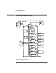
The Analyzer Hardware
purposes. A test bit pattern is sent from the Test and Clock
Synchronization Circuit to the comparator. The comparators then
propagate the test signal on each of the nine channels of the
comparator. Consequently, all data and clock channel pipelines on the
circuit board can be tested by the operating system software from the
comparator.
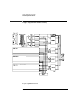
Acquisition
The acquisition circuit is made up of a single Agilent-proprietary ASIC.
Each ASIC is a 34-channel state/timing analyzer, and one such ASIC is
included for every two logic analyzer pods. All of the sequencing,
pattern/range recognition, and event counting functions are performed
on board the IC.
In addition to the storage qualification and counting functions, the
acquisition ASICs also perform master clocking functions. All four state
acquisition clocks are fed to each IC, and the ICs generate their own
sample clocks. Every time you select run, the ICs individually perform
a clock optimization before data is stored.
Clock optimization involves using programmable delays on board the IC
to position the master clock transition where valid data is captured.
This procedure greatly reduces the effects of channel-to-channel skew
and other propagation delays.
In the timing acquisition mode, an oscillator-driven clock circuit
provides a four-phase, 125-MHz clock signal to each of the acquisition
ICs. For high speed timing acquisition (125 MHz and faster), the
sample period is determined by the four-phase, 125-MHz clock signal.
For slower sample rates, one of the acquisition ICs divides the 125-MHz
clock signal to the appropriate sample rate. The sample clock is then
fed to all acquisition ICs.