
User`s guide

Introduction to the Agilent 5500 1
Agilent 5500 SPM User’s Guide 21
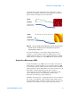
topography. Because the feedback response requires time, constant
current mode is typically slower than constant height mode. However,
greater variations in height can be accommodated.
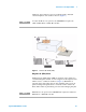
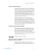
Figure 4 Constant Height mode STM (above) is faster but is limited to
smooth surfaces; Constant Current mode (below) is capable of
mapping larger variation in Z
For electron tunneling to occur, both the sample and tip must be
conductive or semi-conductive. Therefore, STM cannot be used on
insulating materials. This is one of the significant limitations of STM,
which led to the development of other SPM methods described below.
Atomic Force Microscopy (AFM)
Atomic Force Microscopy (AFM) can resolve features as small as an
atomic lattice, for either conductive or non-conductive samples. AFM
provides high-resolution and three-dimensional information, with little
sample preparation. The technique makes it possible to image in-situ, in
fluid, under controlled temperature and in other controlled
environments. The potential of AFM extends to applications in life
science, materials science, electrochemistry, polymer science,
biophysics, nanotechnology, and biotechnology.
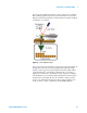
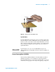
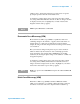
In AFM, as shown in Figure 5, a sharp tip
at the free end of a cantilever
(the “probe”) is brought into contact with the sample surface. The tip
interacts with the surface, causing the cantilever to bend. A laser spot is
reflected from the cantilever onto a position-sensitive photodiode