
User`s guide
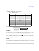


Chapter 1 31
Signal Generator Overview
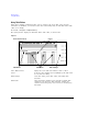
Rear Panel
39. I IN
This female BNC input connector (E8267D only) accepts the in- phase (I) component an externally
supplied, analog, I/Q modulation. The quadrature- phase (Q) component is supplied through the Q IN
connector. The signal level is = 0.5 V
rms
for a calibrated output level. The nominal input
impedance is 50 or 600 ohms. The damage level is 1 V
rms
and 10 V
peak
. To activate signals applied to
the I and Q input connectors, press
Mux > I/Q Source 1 or I/Q Source 2 and then select either Ext 50 Ohm or
Ext 600 Ohm. On signal generators without Option 1EM, this connector is located on the front panel.
40. SYMBOL SYNC
This female BNC input connector (E8267D only) is CMOS- compatible and accepts an externally
supplied symbol sync signal for use with the internal baseband generator (Option 601/602). The
expected input is a 3.3 V CMOS bit clock signal (which is also TTL compatible). SYMBOL SYNC might
occur once per symbol or be a single one-bit-wide pulse that is used to synchronize the first bit of
the first symbol. The maximum clock rate is 50 MHz. The damage levels are > +5.5 V and < −0.5V.
The nominal input impedance is not defined. SYMBOL SYNC can be used in two modes:
• When used as a symbol sync in conjunction with a data clock, the signal must be high during the
first data bit of the symbol. The signal must be valid during the falling edge of the data clock
signal and may be a single pulse or continuous.
• When the SYMBOL SYNC itself is used as the (symbol) clock, the CMOS falling edge is used to
clock the DATA signal.
On signal generators without Option 1EM, this connector is located on the front panel.
41. Q IN
This female BNC input connector (E8267D only) accepts the quadrature- phase (Q) component an
externally supplied, analog, I/Q modulation. The in- phase (I) component is supplied through the I IN
connector. The signal level is = 0.5 V
rms
for a calibrated output level. The nominal input
impedance is 50 or 600 ohms. The damage level is 1 V
rms
and 10 V
peak
. To activate signals applied to
the I and Q input connectors, press
Mux > I/Q Source 1 or I/Q Source 2 and then select either Ext 50 Ohm or
Ext 600 Ohm. On signal generators without Option 1EM, this connector is located on the front panel.
42. DATA
This female BNC input connector (Option 601/602 only) is CMOS compatible and accepts an
externally supplied serial data input for digital modulation applications. The expected input is a 3.3 V
CMOS signal (which is also TTL compatible) where a CMOS high = a data 1 and a CMOS low = a data
0. The maximum input data rate is 50 Mb/s. The data must be valid on the falling edges of the data
clock (normal mode) or the on the falling edges of the symbol sync (symbol mode). The damage levels
are > +5.5 and < −0.5V. The nominal input impedance is not defined. On signal generators without
Option 1EM, this connector is located on the front panel.