FuturePlus Systems Corporation FS2010 Users Manual For use with Agilent Logic Analyzers Revision – 1.
How to reach us ......................................................................................... 4 Product Warranty....................................................................................... 5 Limitation of Warranty ................................................................................... 5 Exclusive Remedies....................................................................................................5 Assistance .........................................................
Use of EyeFinder/Eyescan ............................................................................. 27 Transaction Viewer .................................................................................. 28 General Information................................................................................ 29 Characteristics................................................................................................ 29 State/Timing Adapter Probe Interface Compatibility ...............................
How to reach us For Technical Support: FuturePlus Systems Corporation 36 Olde English Road Bedford NH 03110 TEL: 603-471-2734 FAX: 603-471-2738 On the web http://www.futureplus.com For Sales and Marketing Support: FuturePlus Systems Corporation TEL: 719-278-3540 FAX: 719-278-9586 On the web http://www.futureplus.com FuturePlus Systems has technical sales representatives in several major countries. For an up to date listing please see http://www.futureplus.com/contact.html.
Product Warranty This FuturePlus Systems product has a warranty against defects in material and workmanship for a period of 1 year from the date of shipment. During the warranty period, FuturePlus Systems will, at its option, either replace or repair products proven to be defective. For warranty service or repair, this product must be returned to the factory.
Introduction The FS2010 is a 32/64 bit, 0 to 133Mhz PCI-X State and Timing adapter probe for use with Agilent logic analyzers. This card has a universal card edge connector and a 3.3v extender card connector. The FS2010 PCI-X State/Timing adapter probe and extender card performs three functions. • The first is to act as an extender card, physically extending a module up approximately 1.5 inches from the motherboard connector.
Analyzing the PCI-X Local Bus This chapter introduces you to the FS2010 and lists the minimum equipment required and accessories supplied for PCI-X Local Bus analysis. This chapter also contains information that is common to both state and timing analysis. Accessories Supplied Minimum Equipment Required Additional Equipment Required The FS2010 product consists of the following accessories: • The FS2010 probe.
Signal Naming Conventions This operating manual uses the same signal notation as the PCI-X LOCAL BUS SPECIFICATION - REVISION 1.0 That is, a # symbol at the end of a signal name indicates that the signal’s active state occurs when it is at a low voltage. The absence of a # symbol indicates that the signal is active at a high voltage.
Configuration Files 167xx Analyzer 169xx Analyzer File name for State/Timing Analysis Description 16715/6/7/9 or 1674X or 16750/1/2 1680/90, 16750/1/2, 1691x CP210_1 *2 card state analysis 16715/6/7/9 or 1674X or 16750/1/2 1680/90, 16750/1/2, 1691x CP210_2 *2 card timing 16715/6/7/9 or 1674X or 16750/1/2 1680/90, 16750/1/2, 1691x CP210_3 1 card eyefinder config 16753/4/5/6 16753/4/5/6, 1691x CP210_4 1 card eyescan config *For 32 bit analysis load the timing or state configuration file in
Connecting the 167xx Agilent logic analyzer to the FS2010 The following explains how to connect the logic analyzer to the FS2010 for either state or timing analysis: 1. Connect the logic analyzer PODs 3 adapter cables, either the E5378A or E5385A depending on the logic analyzer cards used. 2. Plug the Adapter cables into the probe as shown in the table below.
Setting up the 167xx Analyzer To install the FS2010 software, insert the diskette labeled 16700/702 Installation disk for the FS2010 into the Agilent 16700 diskette drive. From the SYSTEM ADMINISTRATION TOOLS select INSTALL under SOFTWARE. From the SOFTWARE INSTALL screen select the FLEXIBLE DISK and APPLY. Once the title appears select it and then select INSTALL. This procedure does not need to be repeated. It only needs to be done the first time the PCI-X Analysis Probe is used.
Setting up the 1680/90/900 Analyzer The 1680/90/900 Analyzer is a PC based application that requires a PC running Windows OS with the Agilent logic analyzer software installed or a 16900 frame. Before installing the protocol decoder for the PCI-X protocol on a PC you must install the Agilent logic analyzer software.
Offline Analysis Data that is saved on a 167xx analyzer in fast binary format, or 16900 analyzer data saved as a *.ala file, can be imported into the 1680/90/900 environment for analysis. You can do offline analysis on a PC if you have the 1680/90/900 operating system installed on the PC, if you need this software please contact Agilent. Offline analysis allows a user to be able to analyze a trace offline at a PC so it frees up the analyzer for another person to use the analyzer to capture data.
After clicking “next” you must browse for the fast binary data file you want to import. Once you have located the file and clicked start import, the data should appear in the listing. After the data has been imported you must load the protocol decoder before you will see any decoding. To load the decoder select Tools from the menu bar, when the drop down menu appears select Inverse Assembler, then choose the name of the decoder for your particular product.
After the decoder has loaded, select Preferences if required, from the overview screen and set the preferences to their correct value in order to decode the trace properly. This is a general requirement, some decoders do not have preferences, and if this is the case then no preference setting is necessary.
The Format Menu Label Clk Inputs The FS2010 diskette sets up the format menu as shown in the following table. This format is the same for both Timing and State Analysis.
The PCI-X Transaction Decode Software Loading the configuration file will automatically load the PCI-X Transaction Decode software onto the workspace.
FS2010 Software and Timing mode The FS2010 Decoder should NOT be run when the logic analyzer is configured in timing mode. This will cause the system to hang. The ADDR, ADDR_B and DATA variables The ADDR and DATA variables in the FORMAT menu are assigned to the AD[31:0] signals on the PCI-X bus. The ADDR_B is the AD[63:32] signals on the PCI-X bus.
The CYCLE variable The CYCLE variable is made up of the following signals: TRDY#, FRAME#, IRDY#, C/BE(3:0), DEVSEL# , and STOP#. This variable has 27 symbols defined that can be used to help make triggering, timing analysis and pattern filtering easier. The following lists the bit pattern and the corresponding symbol.
The TERM CODE variable is made up of DEVSEL#, TRDY#, and STOP#. The following lists the bit pattern and the corresponding symbol. Symbol Bit Re-ordering DEVSEL# TRDY# STOP# MASTER ABORT 1 1 1 SPLIT RESPONSE 1 0 1 TARGET ABORT 1 1 0 SINGLE DATA DISC 1 0 0 RETRY 0 1 0 DISC NXT ADB 0 0 0 The hardware layout of the FS2010 made it impossible for the signals to be connected to the logic analyzer in a logical order.
State Analysis This chapter explains how to configure the FS2010 to perform state analysis on the PCI-X Local Bus. The configuration software sets up the format specification menu of the logic analyzer for compatibility with the PCI-X Local Bus. The next chapter explains how to configure the FS2010 to perform timing analysis. The FS2010 State/Timing Adapter Probe interface does not require that a PCI-X add-in card be installed in the FS2010 card edge extender connector.
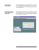
Configuring the Workspace for PCI-X Analysis For full analysis, the PCI-X workspace should appear as below.
The State Listing Display Captured data is as shown in the following figure. The below figure displays the PCI-X transactor decode on a 167xx frame.
T The above figure shows the listing from the 169xx frame.
The FS2010 generates one output column that is sub-divided into the following sub-columns. Name Base CMD TEXT Wait Description The command type displayed in HEX The type of wait state ADDR_H TEXT The address as it appears during a 64 bit address transfer (as defined by a DAC) ADDR_L HEX The address as it appears on the lower AD lines (AD[31:0]).
Timing Analysis Since the FS2010 interface does not buffer the PCI-X bus, it introduces negligible skew to the PCI-X Local Bus signals. Load the logic analyzer configuration file. If the FS2010 software is installed, load the logic analyzer configuration file for timing from the logic/configs/FuturePlus/FS2010 directory on the 167xx analyzer. If using the 1680/90/900 double click the folder that was placed on the desktop during installation and choose the appropriate configuration file.
The Waveform Display Use of EyeFinder/Eyescan Captured data is displayed as shown in the following figure. Use of Eye Finder can greatly enhance your timing analysis by helping find the data valid window of every signal on the bus with respect to the clock. You can compare the results of Eye Finder to your simulation and the PCI-X specification to see if your system operates within expected setup and hold margins. Eye Finder can be found in the setup and hold area of your logic analysis card FORMAT menu.
Transaction Viewer The FS2010 Protocol Decoder version 2.0 or higher is enabled to work with the FuturePlus Systems Transaction Viewer. The Transaction Viewer is a powerful tool that allows the user to view PCI-X data captured with the FS2010 in a graphical environment that presents the information by Transaction as opposed to State. This tool is fully integrated with State Listing on the 16900 and allows marker and trigger settings to be shared between the Protocol Decoder and the Transaction Viewer.
General Information This chapter provides additional reference information including the characteristics and signal connections for the FS2010 module. Characteristics The following operating characteristics are not specifications, but are typical operating characteristics for the FS2010 module. State/Timing Adapter Probe Interface Compatibility 32 or 64 bit PCI-X Local bus universal connector pinout.
Etch length Due to the FS2010 being an interposer all signals are extended 1.2 in. in length, consisting of 57 ohm single-ended impedance etch. Operations All PCI-X Local Bus operations are supported by the hardware and the inverse assembler. Environmental Temperature Operating:0 to 55 degrees C (+32 to +131 degrees F) Altitude Operating: 4,6000m (15,000 ft) Non operating:-40 to +75 degrees C (-40 to +167 degrees F) Non operating: 15,3000m (50,000 ft) Humidity Up to 90% non-condensing.
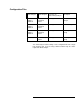
J2 Signal Connector Signal Name/Logical Signal name PCIXCAP DEVSEL# IRDY# AD17 AD19 AD21 AD23 AD25 AD27 AD29 AD31 REQ# NC Logic Analyzer channel number SAMTEC Pin number SAMTEC Pin number Logic Analyzer channel number Ground 1 2 NC 3 4 NC Ground 5 6 Ground Odd D0 7 8 Even D0 Ground 9 10 Ground Odd D1 11 12 Even D1 Ground 13 14 Ground Odd D2 15 16 Even D2 Ground 17 18 Ground Odd D3 19 20 Even D3 Ground 21 22 Ground Odd D4 23 24 Even D4 Ground
Signal Name/Logical Signal name NC INTD# INTB# CLK Ground +5V Logic Analyzer channel number Logic Analyzer channel number Signal name/Logical Signal Name SAMTEC Pin number SAMTEC Pin number Ground 57 58 Ground Odd D13 59 60 Even D13 Ground 61 62 Ground Odd D14 63 64 Even D14 Ground 65 66 Ground Odd D15 67 68 Even D15 Ground 69 70 Ground NC 71 72 NC Ground 73 74 Ground NC 75 76 NC Ground 77 78 Ground Odd D16P/Odd CLKN 79 80 Even DP16P/Even CLKN Grou
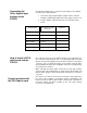
J3 Signal Connections Signal Name/Logical Signal name C/BE4# ACK64# AD1 AD3 AD5 AD7 AD8 NC M66EN AD10 AD12 AD14 C/BE1# Logic Analyzer channel number SAMTEC Pin number SAMTEC Pin number Logic Analyzer channel number Ground 1 2 NC 3 4 NC Ground 5 6 Ground Odd D0 7 8 Even D0 Ground 9 10 Ground Odd D1 11 12 Even D1 Ground 13 14 Ground Odd D2 15 16 Even D2 Ground 17 18 Ground Odd D3 19 20 Even D3 Ground 21 22 Ground Odd D4 23 24 Even D4 Ground 25
Signal Name/Logical Signal name SERR# PERR# LOCK# C/BE2# Ground +5V Logic Analyzer channel number Logic Analyzer channel number Signal name/Logical Signal Name SAMTEC Pin number SAMTEC Pin number Ground 57 58 Ground Odd D13 59 60 Even D13 Ground 61 62 Ground Odd D14 63 64 Even D14 Ground 65 66 Ground Odd D15 67 68 Even D15 Ground 69 70 Ground NC 71 72 NC Ground 73 74 Ground NC 75 76 NC Ground 77 78 Ground Odd D16P/Odd CLKN 79 80 Even DP16P/Even CLKN
J4 Signal Connections Signal Name/Logical Signal name AD33 AD35 AD37 AD39 AD41 AD43 AD45 AD47 C/BE4# AD51 AD53 AD55 AD57 Logic Analyzer channel number SAMTEC Pin number SAMTEC Pin number Logic Analyzer channel number Ground 1 2 NC 3 4 NC Ground 5 6 Ground Odd D0 7 8 Even D0 Ground 9 10 Ground Odd D1 11 12 Even D1 Ground 13 14 Ground Odd D2 15 16 Even D2 Ground 17 18 Ground Odd D3 19 20 Even D3 Ground 21 22 Ground Odd D4 23 24 Even D4 Ground
Signal Name/Logical Signal name AD59 AD61 AD63 C/BE6# Ground +5V Logic Analyzer channel number Logic Analyzer channel number Signal name/Logical Signal Name SAMTEC Pin number SAMTEC Pin number Ground 57 58 Ground Odd D13 59 60 Even D13 Ground 61 62 Ground Odd D14 63 64 Even D14 Ground 65 66 Ground Odd D15 67 68 Even D15 Ground 69 70 Ground NC 71 72 NC Ground 73 74 Ground NC 75 76 NC Ground 77 78 Ground Odd D16P/Odd CLKN 79 80 Even DP16P/Even CLKN G