
Keysigth Technologies N4903B J-BERT

dataTec ▪ Ferdinand-Lassalle-Str. 52 ▪ 72770 Reutlingen ▪ Tel. 07121 / 51 50 50 ▪ Fax 07121 / 51 50 10 ▪ info@datatec.de ▪ www.datatec.de
11
11 | Keysight | J-BERT N4903B High-Performance Serial BERT, 7 Gb/s and 12.5 Gb/s - Data Sheet
Pattern Generator Specications
(continued)
loc output T
loc can operate at full bit-rate or at half bit-rate ption 003 to
support testing of forward cloced devices.
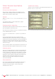
Table 3. loc output specications
Frequency range 150 MHz to 14.2 GHz (Option D14,
in addition to C13 or G13);
150 MHz to 12.5 GHz (Option C13 or G13);
can be programmed up to 13.5 GHz
150 MHz to 7 GHz (Option C07 or G07);
< 620 MHz only with external clock
Half-rate clocking Only with Option 003: Available at bit rates
> 2.7 Gb/s; duty cycle on half-rate clock
adjustable 40% to 60%
Amplitude/resolution 0.050 V pp to 1.800 V pp, 5 mV steps
Output voltage window -2.00 to +3.00 V
Transition times
20% to 80%
10% to 90%
1
< 20 ps
< 25 ps
External termination
voltage
-2 V to +3 V
Jitter 800 fs rms typical with internal clock
SSB phase noise < -75 dBc with internal clock source, 10 GHz
at 10 kHz offset, 1 Hz bandwidth
Interface
3
Differential or single-ended, DC coupled,
50 Ω output ipedance
Connector 2.4 mm female
1. At 10 Gb/s and 7 Gb/s
2. or positive termination voltage or termination to GND external
termination voltage must be less than 3 below . or negative
termination voltage external termination voltage must be less than 2
below . External termination volt age must be less than 3 above
.
3. nused outputs must be terminated with 50 to GND.
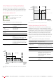
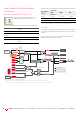
loc input IN
There are two modes when using the cloc input connector.
1. External cloc mode all output signals follow the external
cloc and its modulation. The modulation of the external
cloc must be within the same range given for SS and SJ
see Table 12. If the external cloc is above 6.75 Gz all
internal jitter sources can be used for using 610 ps delay
line external cloc divider z 4. Below 6.75 Gz SJ and
SS are not available. owever the external cloc can
optionally be divided by 1 2 4 8 or 16 provided that the
resulting bit rate does not fall below 150 Mb/s. Modulation
using the 220 ps delay line is still available see igure 22.
2. External P mode it is used to loc the generator to an
external cloc. The provided cloc must not be modulated
in external P mode. All internal jitter sources are
available. A cloc multiplication with x/y is possible with x
y 123 to 255. The resulting bit rate has to be within the
range 620 Mb/s to maximum bit rate.
External clock
10 MHz ref clock
Internal clock
External clock
(PLL mode)
Clock generator
z = 1,2,4,8,16,
resulting bit rate
must be > 150 Mb/s
VCO
VCO
PLL
PLL
1/z
1/z
Clock
source
selection
x/y
igure 16. N4903B supports multiple cloc modes
10 Mz reference input 10 Mz RE IN
This is used to loc the generator to an external 10 Mz reference
cloc. The data rate can be selected within the same range as if
the internal cloc would be used. The provided reference cloc
must not be modulated. All internal jitter sources are available.
Amplitude 200 mV to 2 V
Frequency CLK IN: 150 MHz to 12.5 GHz
(14.2 GHz for Option D14)
10 MHz REF IN: 10 MHz
Interface C coupled, 50 Ω noinal
Connectors
Clock input
10 MHz reference input
SMA female, front panel
BNC, rear panel
Delay control input DEA TR IN
The external signal applied to delay control input varies the delay
between data output and cloc output. This can be used to
generate jittered signals to stress the device under test in
addition to the calibrated jitter injection from N4903B.
Range -110 ps to +110 ps
Sensitivity Typical
Linearity ±5% typical
Modulation bandwidth 1 GHz typical at 10.8 Gb/s data rate
Levels -275 mV to +275 mV
Interface DC coupled, 50 Ω noinal
Connector SMA female
Table 5. Specications for delay control input
Table 4. Specications for cloc input and 10 Mz reference input