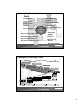
安捷倫科技高頻元件量測研討會 時間: 2006年 2月23日 地點: 高雄金典酒店
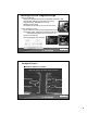
Packaging Development Trend of Integrated Analysis Sung-Mao Wu 安捷倫高頻元件量測研討會 Page 1 2/23/2006 Outline Development Trend for PKG -- PKG Technology Trend -- Why SiP and POP/PIP Challenges to PKG Integrity Design -- Design Challenges on Simulation, Measurement and Design -- Case I : Effective DK -- Case II : Impedance Control verify by TDR -- Case III: TDR FA Application -- Case IV : Substrate Ball Pad Design -- Case V : PDS Analysis Integrated Design -- Components of Optimization PKG Design -- Advanced PKG
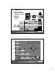
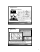
Interesting Semiconductor World Fab/fabless Copper wafer Front/Back end solution Low K material Environment friendly 12” wafer Compact Size Low power consumption Naro meter tech Semiconductor Industry Integrated System Bio tech / New form chip IC/module/System Design Low cost High speed/high frequency Short Time to Market High thermal / Stress solution Worldwide strategy 安捷倫科技高頻元件量測研討會 2/23/2006 Page 3 Packaging Technology Trend Wire Bond Single Chip Package Wire Bond + FC Bond New Intercon
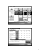
Why SIP ? SoC IC Compare to Board Assembly: MicroPassives SIP Performance Enhancement component Thinner, Smaller, and Lighter Low Cost Compare to SOC Low Cost Memory IC Time to Market Board Assembly Sub-System Flexible Build-up Substrate Single Chip Solution Module SIP Platform Die Stacking Platform Flash SDRAM ASIC Package Stacking Platform Flash SDRAM Flash SDRAM ASIC ASIC 安捷倫科技高頻元件量測研討會 2/23/2006 Page 5 Die Stacking Package Trend • Smaller & Lighter Package Size 0.
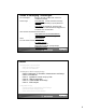
PoP and PiP PoP Package/ Die Count Package Thickness Package Structure 2 PKG/ 3 Chip 2 PKG/ 3 Chip 2 PKG/ 4 Chip 3 PKG/ 7 Chip 1.6 mm Max 1.4 mm Max 1.2 mm Max 2.0 mm Max Flash Flash SDRAM ASIC W/B Type Flash F/C Type SDRAM ASIC Flash SDRAM ASIC SDRAM ASIC PiP 2 PKG/ 3 Chip 2 PKG/ 3 Chip 2 PKG/ 3 Chip 1.4 mm Max 1.2 mm Max 1.
Trends of Packaging Technologies Focus Packages - Bumping, WLCSP, FCBGA, SIP, SCSP and modified LF package Small & Light Thin Thickness in Wafer, Substrate, Package Fine Pitch in Wire Bonding, Flip Chip Bond and Solder Ball High Density by Stacked Die, Package, MultiSubstrate Layer,Substrate Stacked, Staggered Via and Small Trace Via Hole Size - Good Thermal and Electrical Performance Green - High Speed and Low Thermal Resistance Cu / LowLow-K wafer, wafer Nano-technology - Green Solution Low Cos
Challenges to PKG Integrated Design Analysis Challenges ÆMulti-port parameters analysis and broadband calibration skill ÆDouble-side calibration and probing technology ÆSignal-integrity, SSN/SSO and IP drop ÆMixed-signal analysis ÆSubstrate On-line testing, like via, bump and ball…… Design Challenges to SiP ÆPKG selection for different thermal/electrical request ÆSubstrate Design integrated thermal/electrical solution. -- Embedded Die/passive, IPD, decoupling cap…… ÆPKG IP development.
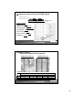
Analysis Case I : ÆMeasurement and ADS setup VNA Long trace short trace Short trace Sample Probe station DUT: (Microstrip/Strip TL) same cross-section with different length 安捷倫科技高頻元件量測研討會 2/23/2006 Page 13 Analysis Case I : Æextraction result 4.5 m4 4.0 3.5 Effective dielectric constant 3.0 2.5 Er_preg Sim/mea comparison 200 m4 freq= 2.358GHz Er_preg=3.828 2.0 1.5 1.0 0.5 0.0 -0.5 -1.0 0 8.00 7.84 7.68 7.52 7.36 7.20 7.04 6.88 6.72 6.56 6.40 6.24 6.08 5.92 5.76 5.60 5.44 5.28 5.12 4.96 4.
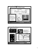
Analysis Case II : ÆImpedance Control Verify by TDR/TDR System Signal Trace in 1st Layer W S T GND Plane in 2nd Layer T1 Dielectric Layer ε= 4.0 Design Condition: Substrate Type : 2 Layer Impedance Control : Differential Simulation Structure : Micro-Strip Line Trace Width (W): 0.39mm Trace Thickness (T): 22 um Dielectric Thickness (T1): 200um Separation (s): 0.
Analysis Case III ÆFA Application ▼ TDR of bare, good, and failure sample bare substrate Open waveform good unit 1 2202 T4 failure Slight difference on the chip capacitance charge curve – A possible reason of this phenomenon is the IMC makes the interface resistance between wire and bond pad growing, which causes the charge current different.
Analysis Case V : PDS Analysis -- Measurement setup 27mm 27mm Top view Bottom view 安捷倫科技高頻元件量測研討會 2/23/2006 Page 19 Analysis Case V : Æ Measurement and Simulation Result (Test Board only) Port 1 Port 2 S21_dB Field propagation @750MHz 安捷倫科技高頻元件量測研討會 2/23/2006 Page 20 10
Analysis Case V : Æcomparison with bare PCB, Package and BGA+PCB Bare PCB Noise coupling between PKG&PCb? package only BGA and PCB Effect of package -5 -10 -15 S21 (dB) -20 -25 -30 -35 -40 -45 -50 -55 0 0.5 1 1.5 2 2.5 3 3.5 4 4.
Components of Optimization Package Design Characterization Lab capability on Electrical, Thermal, Stress and Material Substrate: laminate, build-up, ceramic, RLC embed Design Rule/Spec for substrate layout •Knowing Electrical Characteristics deep inside •Provide package solutions from advanced pkg technology Wire & Bumping Pkg options: structure, cost, thermal, board level... Leadframe: L/F for SOP/QFP etc, L/F for BCC/QFN etc.
Plan and Actions for PKG Design Substrate Design Integrity Electrical Performance -Design Integrity Electrical performance flow -Design Rule and Constraint setting for SiP PKG Application, like RF Module, optical and wireless PKG Active/Passive Device analysis capability -Embedded passive (RF-MEMS, Substrate embedded RLC) analysis and IP-development -Sub-system measurement capability setting for advanced PKG Co-Design and Co-development with key partners -Co-working with key partners for more close and deta
THE END Thank You For Your Listening 安捷倫科技高頻元件量測研討會 2/23/2006 Page 27 14
PNA Based Solutions - Pulsed RF S-Parameter Measurements - Multiport Test Solutions - Physical Layer Test Systems Agilent Technologies Ltd. Ming-Fan, Tsai Project Manager Feb, 23, 2006 安捷倫科技高頻元件量測研討會 Page 1 Feb.23, 2006 Pulsed-RF S-Parameter Applications Using The Agilent PNA Series Network Analyzer 安捷倫科技高頻元件量測研討會 Page 2 Feb.
Agenda • Why Measure in Pulsed Mode and the DUTs We Test – Wafer Test – Power Amplifiers – Antenna RCS – T/R Modules • Review of Pulsed Measurements • Wideband synchronous • Narrowband asynchronous • Evolution of Pulsed VNAs from Agilent • 8510, 85108, 85120, CTS Platform to PNA • Test Sets Available 安捷倫科技高頻元件量測研討會 Feb.
On-Wafer Amplifier Test and Modeling •Most applications are at microwave frequencies •Devices lack adequate heatsinking for CW testing, so pulsed-RF used as a test technique to extract S-parameters •Arbitrary, stable temperature (isothermal state) set by adjusting duty cycle •Duty cycles are typically < 1% •Often requires synchronization of pulsed bias and pulsed RF stimulus 安捷倫科技高頻元件量測研討會 Feb.
Pulsed Antenna Test • About 30% of antenna test involves pulsed-RF stimulus • Test individual antennas, complete systems, or RCS • RCS (Radar Cross Section) measurements often require gating to avoid overloading receiver 安捷倫科技高頻元件量測研討會 Feb.
Radar and Electronic-Warfare •Biggest market for pulsed-RF testing •Traditional applications ≤ 20 GHz •Many now include Multi-Mode Ka-Band •Devices include • amplifiers • T/R modules AN/APG-79 F16C Block 60 • up/down converters Pave-Paws AN/APG-81 JSF 安捷倫科技高頻元件量測研討會 Feb.
VNA Pulsed-RF Measurements VNA data display Magnitude and phase data averaged over duration of pulse data point Frequency domain Average Pulse Swept carrier Data acquired only during specified gate width and position within pulse Frequency domain Point-in-Pulse CW Data acquired at uniformly spaced time positions across pulse (requires a repetitive pulse stream) Pulse Profile dB Magnitude Time domain deg Phase Note: there may not be a one-to-one correlation between data points and the actual n
Pulse-to-Pulse (Single Shot) Measurements • Carrier remains fixed in frequency • Measurement point in pulse remains fixed with respect to pulse trigger (requires wideband detection technique) • One data point for each successive pulse, no pulses skipped • Display magnitude and/or phase versus time One data point for each successive pulse, no pulses skipped CW pulses P1 P2 VNA data display P3 P4 P5 P6 … Time domain 安捷倫科技高頻元件量測研討會 Feb.
Typical Hardware Setup For Wideband Detection Point-in-Pulse and Pulse-to-Pulse External pulse generator (e.g., 81110A/81111A) Output 1 PNA (20, 40, 50, or 67 GHz) with: • 014 Configurable test set • UNL Source attenuators • 080 Frequency offset mode To TRIG IN (rear panel) 10 MHz Ref Output 2 Cplr Thru Src Out Ref In Z5623A H81 2-20 GHz RF modulator DUT Note: pulse generator controls timing Additional PNA setup: • step sweep • frequency offset on (0 Hz) • Auto IF gain = off 安捷倫科技高頻元件量測研討會 Feb.
Minimum Pulse Widths for Point-in-Pulse Measurements Using Wideband Detection Maximum IF bandwidth Minimum pulse width IF auto-gain mode* PNA models (20, 40, 50, 67 GHz) 40 kHz 50 us Yes PNA-L models (2-port, 20, 40, 50 GHz) 250 kHz 10 us Yes PNA-L models (2-port, 6, 13.5 GHz; 4-port, 20 GHz) 600 kHz 2 us No * Note: for point-in-pulse measurements, the IF auto-gain mode should be turned off (i.e., set IF gains manually) 安捷倫科技高頻元件量測研討會 Feb.
Pulsed S-parameter Measurement Modes Narrowband/asynchronous acquisition • Extract central spectral component only; measurement appears CW • Data acquisition is not synchronized with incoming pulses (pulse trigger not required) • Sometimes called “high PRF” since normally, PRF >> IF bandwidth • “Spectral nulling" technique achieves wider bandwidths and faster measurements • No lower limit to pulse width, but dynamic range is function of duty cycle IF filter Time domain IF filter D/R degradation = 20*log[d
Typical Hardware Setup (Narrowband) External pulse generator (e.g.
85108A First True pulsed Network Analyser Still the most widely used system for TR Module R&D and manufacturing test (>100 off world-wide still in use) Wholly COTS solution Affordable Low cost of ownership Low risk Point-on-pulse Pulse profile, repetitive 安捷倫科技高頻元件量測研討會 Feb.23, 2006 Page 23 Pulsed PNA is the New Generation 85108A COTS stand alone hardware can perform: – Point-on-pulse – Pulse-to-Pulse – Pulse profile Timing generator can trigger custom user hardware e.g.
Comparing the 8510 and PNA 8510 (85108A) • Dominant mode is wideband detection • Detection is done BEFORE analog-to-digital conversion • Analog synchronous detector produces baseband I/Q output (detector bandwidth = 1.
Agilent TR Module Test Systems continued CTS-I Family CTS-II Family 安捷倫科技高頻元件量測研討會 Feb.
Agenda • Why Measure in Pulsed Mode and the DUTs We Test – Wafer Test – Power Amplifiers – Antenna RCS – T/R Modules • Review of Pulsed Measurements • Wideband synchronous • Narrowband asynchronous • Evolution of Pulsed VNAs from Agilent • 8510, 85108, 85120, CTS Platform to PNA • Test Sets Available 安捷倫科技高頻元件量測研討會 Feb.
PNA Pulsed-RF Configuration Example 1 • User-supplied external modulator • Average pulse measurements 81110A family pulse generator Advantage: simplest – use any standard PNA with 014 GPIB Pulse out 10MHz Ref Src Out Power Supply Cplr Thru RF in Com +25 -25 RF out TTL DC(+) DC(-) 安捷倫科技高頻元件量測研討會 Feb.
PNA Pulsed-RF Configuration Example 3: Full Forward/Reverse S-Parameter Configuration 81110A family pulse generators GPIB One output channel drives RF modulator Trigger 10 MHz Ref Three output channels drive internal receiver gates A, B, and R1/R2 for pointin-pulse and pulse-profile measurements PNA DUT 安捷倫科技高頻元件量測研討會 Page 33 Feb.23, 2006 PNA Pulsed-RF Configuration Example 3: Full Forward/Reverse S-Parameter Configuration a different view 安捷倫科技高頻元件量測研討會 Page 34 Feb.
Z5623A H83 – H84 Test Set Control Macro 安捷倫科技高頻元件量測研討會 Feb.
PNA Pulsed-RF Configuration Example 4 • Modulator test set, external receiver gate • Point-in-pulse, pulse profile 81110A family pulse generator GPIB Advantage: gate widths < 20 ns Pulse1 out 10 MHz Ref Pulse2 out Src Out External switch in receiver B loop for external gating Ref In TTL Power Supply Com +25 -25 DC(+) DC(-) Z5623A H81 pulsed-RF test set 安捷倫科技高頻元件量測研討會 Feb.
PNA Pulsed-RF Configuration Example 6 • Customer-supplied pulsed bias and pulsed RF, internal IF gate • Point-in-pulse, pulse profile 81110A family pulse generators GPIB Trigger Pulse1 out Advantage: both pulsed bias and pulsed-RF stimulus 10 MHz Ref Src Out Pulse3 drive to internal receiver gate B (for point-inpulse) Cplr Thru RF in Power Supply RF out Pulse2 out TTL DC(-) Com +25 -25 DC(+) 安捷倫科技高頻元件量測研討會 Feb.
Resources • www.agilent.com/find/pulsedrf 安捷倫科技高頻元件量測研討會 Page 41 Feb.23, 2006 Multiport - PNA based solutions 安捷倫科技高頻元件量測研討會 Page 42 Feb.
Agenda • Target Applications • PNA Multiport Test Solutions • Specials vs. Standard product • Customer data required for new multiport specials • Further Information 安捷倫科技高頻元件量測研討會 Feb.23, 2006 Page 43 Target Applications • Front End Module (FEM) • Cellular FEM (see next slide) • WLAN FEM (Base Band not included, 2.
Cellular FEM #1 (Dual band, 1xEV,GPS) Diversity Rx 安捷倫科技高頻元件量測研討會 Page 45 Feb.23, 2006 Cellular FEM #2 (Quad band, UMTS,GSM) 安捷倫科技高頻元件量測研討會 Page 46 Feb.
WLAN FEM(2.4G・5G dual band) 2.4 GHz / 5 GHz WLAN FEM BPF 2.4 GHz Rx 5 GHz Rx LNA 2.4 GHz Tx Diversity SW 5 GHz Tx Diplexer PA 安捷倫科技高頻元件量測研討會 Feb.23, 2006 Page 47 Multiport & High Power Testing Devices • Typical High Frequency devices – Switches, Couplers, Power Splitter/Divider and etc.. – Filter/Coupler array • Multiport and high power – PA Cellular/WLAN FEM with PA – RF switch IC ( Switch filters) 安捷倫科技高頻元件量測研討會 Page 48 Feb.
Key Measurement Requirements Cellular FEM without PA • IL, RL for each path up 12.75GHz • Isolation – Frequency > 3x Carrier – Signal level 0dBm or –10dBm • Switch distortion – Frequency up to 12.75GHz in R&D – Signal Level up +36dBm UMTS850 UMTS1900 GSM Tx 安捷倫科技高頻元件量測研討會 Feb.23, 2006 Page 49 Key Measurement Requirements BPF WLAN FEM with PA – – – – Gain, 1dB Compression, Pout,PAE RL Isolation Harmonics distortion • Frequency Cellular > 3x Carrier Frequency • Frequency(WLAN): 17.
Agenda • Target Applications • PNA Multiport Test Solutions • Specials vs. Standard product • Customer data required for new multiport specials • Further Information 安捷倫科技高頻元件量測研討會 Feb.23, 2006 Page 51 New PNA Rev 6.
PNA/PNA-L Option 550 Measure SParameter Balanced Receivers Applications • New firmware option 550 for the PNA/PNA-L adds full 4port capability and differential measurements to a two port network analyzer • CPL Dec 1, 2005 • $7k RFP 安捷倫科技高頻元件量測研討會 Feb.23, 2006 Page 53 Variety Summary Switching Extension Hybrid Special Multiport Test Varieties SCMM Signal Conditioning 安捷倫科技高頻元件量測研討會 Page 54 Feb.
Test Sets Overview Platform Description Benefits 87050A-Hxx/Kxx Switching test sets. Lower cost No coupler inside test set N4419/20/21B/H67 Extension test sets 4-port differential to 67Ghz Coupler on each port Z5623A-Hxx/Kxx Depend on the particular option Meets customer specific req’ts Mixing of Switching and Extension test sets 安捷倫科技高頻元件量測研討會 Feb.23, 2006 Page 55 Agilent’s Promoted Multiport Products & Specials 安捷倫科技高頻元件量測研討會 Page 56 Feb.
Agilent PNA > 4-port Products offering Freq. Coverage: PNA Based Unit & Ext. Test set Total Test Ports 300 KHz – 20 GHz N5230A opt. 245 & Z5623AK64 6 300 KHz – 20 GHz N5230A opt. 245 & Z5623AK66 14 300 KHz – 20 GHz N5230A opt. 245 & Z5623AKxx 20 .010 – 40GHz E8363/4B or E8361A & 87050A-K62* 6 * 2-port cal only 安捷倫科技高頻元件量測研討會 Page 57 Feb.
Multiport Specials – Variety • Hybrid Test Sets – Hybrid test sets are a combination of the switching and extension types. Test ports can be either switched or coupler bridge based. 安捷倫科技高頻元件量測研討會 Feb.23, 2006 Page 59 Multiport Specials – Variety • Switching Test Sets GPIB J1 – Switching test sets provide signal paths from the network analyzer test ports to the DUT.
Multiport Specials – Variety • SCMM – Single connection multiple measurement test sets allow the user to make different types of measurements with out having to disconnect there DUT form the test set.
Agenda • Target Applications • PNA Multiport Test Solutions • Specials vs. Standard product • Customer data required for new multiport specials • Further Information 安捷倫科技高頻元件量測研討會 Feb.
Multiport Specials –Specials vs. Standard product Multiport Special – Custom – Does not follow the NPI PLC process – Fast development to shipment – Typical supplemental performance – Provide just enough performance • Functional Certificate • Return to Factory support Standard Product – Follows the NPI PLC process – Specifications with uncertainties. – Box and System level performance • Calibration Certificate • Return to Bench support • Verification test 安捷倫科技高頻元件量測研討會 Feb.
Agenda • Target Applications • PNA Multiport Test Solutions • Specials vs. Standard product • Customer data required for new multiport specials • Further Information 安捷倫科技高頻元件量測研討會 Feb.
Agenda • Target Applications • PNA Multiport Test Solutions • Specials vs. Standard product • Customer data required for new multiport specials • Further Information 安捷倫科技高頻元件量測研討會 Feb.23, 2006 Page 69 Information Sources Freq. Coverage: 300 KHz – 20 GHz 300 KHz – 20 GHz .45 – 20/40/50 GHz .45 – 67.0 GHz Ext. Test Set & #Ports Z5623AK64 2-port Z5623AK66 10-port N4419/20/21B 2-port N4421BH67 2-port ¾ http://mktwww.soco.agilent.com/Product-Info/Network-Analyzers/PNA/multiport.htm ¾ http://www.agilent.
Summary • PNA multiport test solutions provide: – Direct test set control made easy with PNA Firmware Rev 6.0s – Flexible test port configuration that enables customer to perform variety kinds of multiport device measurements – Advanced measurement capabilities, such as the APE, result in accurate measurements 安捷倫科技高頻元件量測研討會 Feb.23, 2006 Page 71 Complete Characterization of Backplane Differential Channels February 23, 2006 presented by: Ming-Fan, Tsai Agilent Technologies Ltd.
Overview Backplanes Measurement set up Single-ended Differential Frequency & time domain Eye diagrams Model extraction 安捷倫科技高頻元件量測研討會 Feb.23, 2006 Page 73 All Next Generation High Speed Serial Links will use Differential Signaling Serial ATA 1.25 Gbps Hypertransport 1.6 Gbps AGP8x 2.1 Gbps Infiniband 2.5 Gbps PCI Express 2.5 Gbps Serial ATA II 2.5 Gbps XAUI 3.125 Gbps PCI Express II 5.0 Gbps OC-192 9.953 Gbps 10 GbE 10 Gbps OC-768 39.81 Gbps 安捷倫科技高頻元件量測研討會 Page 74 Feb.
Important Physical Layer Properties of Differential Channels Differential impedance profile (diff return loss) Transmitted differential signal quality (diff insertion loss) Conversion of differential to common signal Where conversion of differential to common signal occurs Eye diagrams (1 Gbps Æ 10 Gbps) 安捷倫科技高頻元件量測研討會 Feb.
Differential VNA/TDR Applied to All Passive, Linear Components and Interconnects z When an external precision signal is required z Applies to any passive interconnect or component z z z z z z Backplanes Discretes Packages Connectors PCB structures Material properties 安捷倫科技高頻元件量測研討會 Feb.23, 2006 Page 77 A Precision Instrument is Not Enough! Component to characterize ? Instrument ? Valuable information 安捷倫科技高頻元件量測研討會 Page 78 Feb.
Complete Characterization System Solution DUT + microprobes GigaTest Probe Station Physical Layer Test System: VNA + PLTS software 安捷倫科技高頻元件量測研討會 Feb.23, 2006 Page 79 Microprobes Allow Precision Probing of Structures with Minimal Artifacts Close up Pitch ~ 50µ – 1000µ 安捷倫科技高頻元件量測研討會 Page 80 Feb.
4 Port Differential VNA Techniques Applied to Tyco Electronics HM-Zd Legacy Backplane System Total channel lengths: 26 inches, 40 inches 2 inches, daughter card 2 inches, daughter card 16 inches, 30 inches backplane 安捷倫科技高頻元件量測研討會 Feb.
TDR and VNA Techniques t TDR t S11 Incident wave ed lect Ref e wa v Incident wave w ed lect f e R Transmitted wave TDT Transmitted wave S21 DUT DUT ave 安捷倫科技高頻元件量測研討會 Feb.23, 2006 Page 83 4 Port, Single-ended S-parameters: Tyco Backplane Example Interpreting single ended measurements: S11 : return loss, single ended S21= S12 : insertion loss, single ended S31= S13 : near end cross talk S41= S14 : far end cross talk 安捷倫科技高頻元件量測研討會 Page 84 Feb.
Single-ended Return Loss and Insertion Loss: 26 inch channel length Input Single-ended Return Loss S11 Input Single-ended Insertion Loss S21 0 dB -10 dB -20 dB -30 dB 2 GHz/div -40 dB -50 dB 2 GHz/div 安捷倫科技高頻元件量測研討會 Page 85 Feb.23, 2006 Microprobing on SMA Pads Added ground pad 安捷倫科技高頻元件量測研討會 Page 86 Feb.
Bandwidth Limit of SMA vs. Microprobes 0 dB S11- return loss Measured with SMA connector -10 dB Measured with microprobe -20 dB Conclusions: -30 dB 1. Microprobes can be higher bandwidth (important > 14 GHz) 2. Identical performance < 10 GHz for these SMA connectors -40 dB -50 dB 20 GHz full scale 安捷倫科技高頻元件量測研討會 Feb.
Microprobing vs. SMA Connectors Strengths SMA Connectors • No additional fixturing to VNA required • Easy to use • Mechanically robust Micro Probes Weaknesses • Can’t use on functional boards- loads the line too much • Limited density • Can use on any signal lines • Probe station required • No constraints on how many or where • Probes can be damaged • Can be used on functional board • Important for active probing 安捷倫科技高頻元件量測研討會 Feb.
4 Port Balanced Measurements: Frequency and Time Domain Differential Single-ended 1 3 Diff pair port 1 2 (and their return paths!) Diff pair port 2 (and their return paths!) 4 Stimulus Differential Signal Response Stimulus S11 S21 S31 S 41 S12 S 22 S 32 S 42 S13 S 23 S33 S 43 S14 S 24 S 34 S 44 Common Signal Port 1 Port 2 Port 1 Port 2 SDD11 SDD21 SCD11 SCD21 SDD12 SDD22 SCD12 SCD22 SDC11 SDC21 SCC11 SCC21 SDC12 SDC22 SCC12 SCC22 安捷倫科技高頻元件量測研討會 Feb.
Important Performance Terms Diff pair port 1 Diff pair port 2 (and their return paths!) Stimulus Differential Signal Port 1 SDD11 SDD21 SCD11 SCD21 Port 2 SDD12 SDD22 SCD12 S CD22 SDD11 differential impedance profile SDD21 Signal quality of differential signal, time delay of differential signal SCD21 Conversion of differential signal to common signal in transmission (emissions) SDC21 Conversion of common signal to differential signal in transmission (susceptibility) SCC11 Common impedance pr
Differential Return Loss & Reflection Coefficient 0 dB-- Frequency Domain SDD11 Time Domain TDD11 t=0 1 nsec/div 120 Ω− 100 Ω− 80 Ω− 20 GHz full scale -50 dB-Conclusions -Connectors create large impedance discontinuity -Daughter card differential impedance is 110 Ω -Backplane differential impedance is 102 Ω 安捷倫科技高頻元件量測研討會 Feb.
Important Design Feedback Designing for 50 Ohm single ended line is not the same as a 100 Ohm differential line. Characterizing with single ended TDR will not measure differential impedance. Design the daughter cards with as much care as the backplane. Most discontinuities from connectors are not from the connectors- they are from the via fields. Optimizing connectors is all about optimizing the circuit board via field layout. Design for test: add copper fills for microprobing 安捷倫科技高頻元件量測研討會 Feb.
Differential Transmitted Signal SDD21 Frequency Domain SDD21 0 dB-Conclusions: -10 dB-- • Measurement system bandwidth > 40 GHz -20 dB-- 26 inch backplane trace 40 inch backplane trace • 26 inch traces have a 15 dB BW ~ 3.5 GHz • 40 inch traces have a 15 dB BW ~ 2 GHz 10 GHz full scale -100 dB-- 安捷倫科技高頻元件量測研討會 Feb.
Eye Diagrams: 26 inch Channel 1 Gbps, 200 psec/div 2.5 Gbps, 80 psec/div 5 Gbps, 40 psec/div 7.5 Gbps, 27 psec/div 安捷倫科技高頻元件量測研討會 Feb.
Differential Signal Input Æ Common Signal Output 26 inch channel length TDD21 ~7% of differential signal amplitude converted to common signal TCD21, 20x scale May be a problem if it were on CAT5 twisted pair 1 nsec/div 安捷倫科技高頻元件量測研討會 Feb.23, 2006 Page 103 Where did the Conversion Happen? TDD11 TCD11 x10 scale increase Conclusion: most mode conversion happens in the via fields! asymmetry of backplane traces Via field on daughter card Via field on mother board 安捷倫科技高頻元件量測研討會 Page 104 Feb.
Measurement and Model Extraction TIME DOMAIN SIMULATORS (HSPICE®, SPECTRAQUEST®, SMARTSPICE) BEHAVRIOAL MODELS S-PARAMETERS TOPOLOGICAL MODELS FREQUENCY-DOMAIN SIMULATORS (ADS, ETC) TDA SYSTEMS ICONNECT MEASUREXTRACTOR Note TIME DOMAIN S-PARAMETERS AGILENT TECHNOLOGIES N1900-SERIES PHYSICAL LAYER TEST SYSTEM TDR or VNA AGILENT TECHNOLOGIES PNA SERIES VECTOR NETWORK ANALYZERS AGILENT TECHNOLOGIES 86100-SERIES TIME DOMAIN REFLECTOMETERS See Note DEVICE UNDER TEST DEVICE UNDER TEST Page 105 Not
Conclusions Differential pairs will proliferate Differential characterization requires • • • • microprobes probe station 4 port VNA Analysis software Absolutely everything you ever wanted to know about the performance of a differential pair is contained in the 4 port balanced S parametersdisplayed in either the frequency or time domain 安捷倫科技高頻元件量測研討會 Feb.23, 2006 Page 107 Technical Information Resources Visit www.gigatest.com for..
FREE Agilent Email Updates Subscribe Today! Choose the information YOU want. Change your preferences or unsubscribe anytime. Keep up to date on: Services and Support Information Events and Announcement - Firmware updates - New product announcement - Manuals - Technology information - Education and training courses - Application and product notes - Calibration - Seminars and Tradeshows - Additional services - eSeminars Visit: www.agilent.com/find/eseminar-email 安捷倫科技高頻元件量測研討會 Page 109 Feb.
Enhanced TDR Channel Characterization Capabilities Agilent Technologies Ltd. Brian Chi Senior Project Manager Agilent Technologies brian-tn_chi@agilent.com 03-4959054 Feb, 23, 2006 安捷倫科技高頻元件量測研討會 Page 1 Feb.23, 2006 Impedance in Time Domain Z Impedance? High Speed Digital Design 安捷倫科技高頻元件量測研討會 Page 2 Feb.
Impedance in Time Domain Short Termination PROBE R 0Ω E What do you expect to see at the probe before, during, and after you close the switch? E E/2 0 Time 安捷倫科技高頻元件量測研討會 Feb.23, 2006 Page 3 Impedance in Time Domain Open Termination PROBE R E ∞Ω What do you expect to see at the probe before, during, and after you close the switch? E E/2 0 Time 安捷倫科技高頻元件量測研討會 Page 4 Feb.
Impedance in Time Domain Perfect Termination PROBE R R E What do you expect to see at the probe before, during, and after you close the switch? E E/2 0 Time 安捷倫科技高頻元件量測研討會 Feb.23, 2006 Page 5 Impedance in Time Domain Impedance Mismatch Terms Z L = Z0 1+ ρ 1− ρ ρ= (∆V) E Vr E/2 0 Vr Vi Vi Time Impedance Calculated from Source Impedance and Reflection Coefficient. Reflection Coefficient: How much was reflected? ∞Ω ZL=Z0 Ω Vr Zero Ω 安捷倫科技高頻元件量測研討會 Page 6 Feb.
Impedance in Time Domain Mismatch Exercise PROBE Z0 = 50 Ω Vi = 200 mV R Vr = 66.6 mV ? E ZL = ? What is the value of ΖL? Vr(ΔV) Vi 200 mVolts 66.6 mV 200 mV 0 Volts Time 安捷倫科技高頻元件量測研討會 Feb.23, 2006 Page 7 Step Reflection Testing OSCILLOSCOPE Ei Er ZL TRANSMISSION SYSTEM UNDER TEST Er STEP GENERATOR Typical Step: 200 mV, 25 kHz square wave with 35 ps rise time Ei T Oscilloscope display when Er ≠ 0 安捷倫科技高頻元件量測研討會 Page 8 Feb.
Mismatches Location Distance Formula Where νp = velocity of propagation T D =υp ⋅ 2 T = transit time from monitoring point to the mismatch and back Why is the transit time divided by two? ZL 安捷倫科技高頻元件量測研討會 Feb.
Simple Loads Reflection Analyzing The shape of the reflected wave reveals the nature and magnitude of the mismatch Z=? 0< ZL − Z0 < +1 ZL + Z0 What is the nature of each of the loads shown at the right? a) SHORT b) OPEN c) IMPEDANCE > Z0 d) IMPEDANCE < Z0 Z=? −1< ZL − Z0 <0 ZL + Z0 安捷倫科技高頻元件量測研討會 Feb.
Complex Loads Reflection Analyzing The shape of the reflected wave reveals the nature and magnitude of the reflection Complex load impedances are also identified Series R-C Shunt R-C R C R C 安捷倫科技高頻元件量測研討會 Page 13 Feb.23, 2006 Analyzing Reflections of Complex Loads 安捷倫科技高頻元件量測研討會 Page 14 Feb.
Analyzing Reflections of Complex Loads 安捷倫科技高頻元件量測研討會 Feb.23, 2006 Page 15 Z DUT = Z 0 Vincident + Vreflected Vmeasured = Z0 Vincident − Vreflected 2 • Vincident − Vmeasured 安捷倫科技高頻元件量測研討會 Page 16 Feb.
Required Parameters by Standard – S Standard Max Freq, Impedance Return Loss Loss parameters GHz PCI Express Gen 2 PCI Express PCI-X Serial Attached SCSI IPC Fully Buffered DIMM IEEE 802.3ae Infiniband Serial ATA EIA-364-90 EIA-108 HDMI DVI Firewire USB 2.0 RapidIO 5 1.25 7.5 N/A 2.4 ? 6.3 4.5 N/A N/A 4.1 4.1 8 1.
Introducing 86100C option 202 - Corrected Impedance Profile - Peeling Peeling mitigate measurement errors caused by multiple reflections at each impedance mismatch. Blue: raw data Yellow : corrected 安捷倫科技高頻元件量測研討會 Feb.23, 2006 Page 19 Matching source Z0 to transmission line ZL WHAT IF THE TRANSMISSION LINE OR CABLE DOES NOT MATCH THE SOURCE IMPEDANCE? WHAT WILL THE RESPONSE LOOK LIKE? E 50 75 ∞ 安捷倫科技高頻元件量測研討會 Page 20 Feb.
Peeling - Voltage Bounce Diagram source 50Ω 75Ω ΓS = - 0.2 -Γl = - 0.2 Open 50Ω Raw Voltage ΓR = = 1.0 240 mV t=0 240 mV 192 mV -48 mV 9.6 mV 192 mV 201.6 mV t=2 (192 –1.92)mV t=4 Peeled Voltage 383 mV Keeps on approaching steady state of 400 mV 安捷倫科技高頻元件量測研討會 Feb.23, 2006 Page 21 Corrected Z Profile into a 75 Ω Cable Peeling assumes Loss-less device. Loss, Resistance [R], degrade accuracy of peeling. Initial Z mismatch is the most accurate.
TDR normalization (As VNA’s Calibration) What is Normalization? • Built-in Firmware • Removes Test Fixture Error • Increases Accuracy • Allows Customer to Simulate his own system risetime Originally Licensed from Stanford University (Bracewell Transform) Critical for Rambus! 安捷倫科技高頻元件量測研討會 Feb.
The procedure of TDR Normalization 安捷倫科技高頻元件量測研討會 Feb.23, 2006 Page 25 Effect of TDR Normalization Calibration Fixture DUT Reference plane by Calibration Remove Error caused by Test Fixture, Cable, connectors 安捷倫科技高頻元件量測研討會 Page 26 Feb.
Fixture Error Correction Techniques TDR Peeling Measurement Goals By VNA •Accuracy •Repeatability •High Dynamic range •Complete characterization = Post-measurement process Source : DesignCon 2005 “Designing Transceiver FPGA's Using Advanced Calibration Techniques” = Pre-measurement process 安捷倫科技高頻元件量測研討會 Feb.
Comparison of TDR and PNA (Error Correction) Good Calibration yields ~1dB error below 10GHz Magnitude Phase PNA RPC Norm@20pS Norm@30pS TDR Waveforms @30pS RPC @20pS & PNA Comparison: TDR Calibration Methods versus PNA SOLT Calibration Device Under Test: 3.5 mm Thru Adapter Results: The magnitude loss increases as a function of frequency and is dependent upon the calibration method for TDR-based measurements. Phase error due to timing jitter exists in TDRbased measurements. 安捷倫科技高頻元件量測研討會 Feb.
TDR vs VNA comparison Mismatch Line Device #1 Return Loss S11 (Magnitude dB) 50MHz 5.00E+07 10GHz 2.54E+09 5.04E+09 7.53E+09 1.00E+10 20GHz 1.25E+10 1.50E+10 1.75E+10 2.00E+10 0 0 -5 -5 -10 -10 -15 -15 VNA -20 -20 -25 -25 -30 -30 -35 -35 TDR 安捷倫科技高頻元件量測研討會 Feb.23, 2006 Page 31 N1024A TDR Calibration Kit Best for Differential normalization 2 x Loads and 2 x Shorts Current 54754A-100 Accessory 3 36” SMA cables Kit 1 SMA-f load 1 SMA-m load 1 SMA-f short 2 SMA-m to BNC-f 5 3.
Diff. TDR Probe Used for handheld Differential meas. 2 x Diff. and 2 x Single Ended Probes Current 54754A-100 Accessory 3 36” SMA cables Kit 1 SMA-f load 1 SMA-m load 1 SMA-f short 2 SMA-m to BNC-f 5 3.5mm 20dB pads PS-X10-100 2 2 2 2 2 1 1 1 SMA cables SMA-m precision load SMA-m flush short Size Diff. TDR probe Size Single Ended Probe Calibration Subtract Hand Held holder ESD protection (option) 安捷倫科技高頻元件量測研討會 Feb.
On Wafer & Packages measuring example 安捷倫科技高頻元件量測研討會 Page 35 Feb.23, 2006 Interconnects – Using Excess L/C 安捷倫科技高頻元件量測研討會 Page 36 Feb.
How close can two reflection sites be and still be seen as independent events? The TDR edge needs time to reach its full height before the next event is encountered So what determines the two-event resolution? Answer: It’s not just the TDR step speed! 安捷倫科技高頻元件量測研討會 Feb.23, 2006 Page 37 A 35 picosecond step is insufficient to see closely spaced reflections With a 35 ps step, all you know is the device is there If there is more than one reflection, we can’t tell 35ps 安捷倫科技高頻元件量測研討會 Page 38 Feb.
High resolution allows your customers to see what they could never see before hermetic feedthrough 9ps V-connector pin-collette coaxial feedthrough V-connector pin-collette coaxialmicrostrip launch microstrip transmission line At 9 ps step speed, we see 5 separate reflections Each event is easily seen and quantified 安捷倫科技高頻元件量測研討會 Feb.
Optimizing Measurements 54754A TDR module 86118A You will lose your edge speed if you have: • Excess or poor quality cabling to and from the DUT Sampling Port • The scope receiver channel has insufficient BW Recommend TDR with the 86118A ~75 GHz remote plugin: 4020 Remote TDR Head • Max. bandwidth • Minimum cabling distances • Connector recommend as 2.4mm Device Under Test 安捷倫科技高頻元件量測研討會 Page 41 Feb.
Physical Layer Test System (PLTS) is the Most Complete for Differential S parameters •Extensive Calibration •Eye diagram simulation •N5320A-225 20G VNA •N5320A-240 20G VNA •54754Ax2 TDR base 安捷倫科技高頻元件量測研討會 Page 43 Feb.23, 2006 安捷倫科技高頻元件量測研討會 Page 44 Feb.
Using ADS for Signal Integrity Design Signal Integrity and Advanced Design System Agilent Technologies Ltd. Ming Chih, Lin Application Engineer Feb, 23, 2006 安捷倫科技高頻元件量測研討會 Page 1 Feb.23, 2006 Overview Part I • Unified Environment for SI Design Part II • Application Guides for SI • Eye Diagram • IBIS Model • Momentum 安捷倫科技高頻元件量測研討會 Page 2 Feb.
Using ADS for Signal Integrity Design Unified Environment for SI Design 安捷倫科技高頻元件量測研討會 Page 3 Feb.23, 2006 Signal Integrity Problems are Everywhere! Wafers Backplanes PC Boards IC Packages Cables 安捷倫科技高頻元件量測研討會 Page 4 Feb.
Signal Integrity (SI)- What is it? “Signal integrity is a field of study half-way between digital design and analog circuit theory” Dr. Howard Johnson It is the application of engineering principles to: Control impedance and reflections Minimize parasitic and unwanted coupling effects Control skew Adjust for skin-effect and dielectric losses Transmitter Pre-emphasis Receiver Equalization So chips can communicate at higher data rates 安捷倫科技高頻元件量測研討會 Feb.
Computer Interconnect Standards Second gen PCI-Express (5-6.25Gb/s) 10Gb Ethernet 6Gb/s SATA III VXS Backplane (VITA41) 6.25Gb/s double XAUI GigE Backplane (VITA 31.1) AdvancedTCA (PICMG 3.x) 5.0Gb/s Serial Mesh Backplane (PICMG 2.20) XAUI 3.125Gb/s RapidIO 3.0Gb/s 3.125Gb/s 3GIO/PCI-Express 2.5Gb/s InfiniBand 2.5Gb/s 2.5Gb/s Fibre-Channel Flexbus 4 POS-PHY L3/L4 IEEE 1394 CSIX VME USB CompactPCI SCSI 1.6Gb/s PCI-X 66 & 100 XAUI 2.
Agilent’s Signal Integrity Solutions 安捷倫科技高頻元件量測研討會 Feb.
Agilent – 20 years of Simulation Innovation RFIC From Touchstone to ADS stem n Sy High YEAR ve owa ra, Micr & Lib tone s h c u f To EEso 198 0 d dig ital MDS ies IV , Ser e my d a c 1990 A Layout-driven simulation Yield Optimization Wireless Design Libraries Discrete-valued Optimization Phase-noise Analysis Ptolemy Timesynchronous Dataflow Simulator High-Frequency SPICE Optimization from Layout MDS for Unix Harmonic Balance Simulator Standards-based Communications Libraries Transient-assisted
4-port Measurement of Connector 安捷倫科技高頻元件量測研討會 Feb.23, 2006 Page 13 Simulated Step-response of Measured Connector •Differential pair simulated their response to a voltage step. •Main through line is held fixed during simulation 600 • The complement line is swept from +/-50ps 400 200 Vport4, mV Vport2, mV • magnetic effect in board is evident in measurement. differential, true/complement skew +/- 50 ps. Both output steps shown Below. 0 -200 -400 -600 0.4 0.5 0.6 0.7 0.8 0.9 1.
Simulated Eye Diagram of Measured Connector Differential, true/compliment skew +/- 50 ps • Eye opening on left-side is smaller than on right-side of crossing point for –50, -40, 30ps. • Jitter is higher for – 50, -40 and -30 ps eyes • Slope of rise is shallower for + and – 50 ps eyes • Eye opening is balanced and and rise is faster for 0, +10 and +20ps • Physical line added to board to adjust delay based on these results 安捷倫科技高頻元件量測研討會 Feb.
ADS for Signal Integrity – Link Level Simulation Channel Adaptation Simulators • • • • • Frequency-domain Time-domain Numeric Domain 3-D Planar Electromagnetic 3-D Electromagnetic • • • • • • Optimized equivalent circuit models Analytic transmission line models Static field-solver based models EM simulation models Models from measurements Matlab, VHDL, C++, SystemC, Verilog_A Measurements • TDR and TDT • 2-port and 4-port VNA • Eye Diagram Encoder Pre-emphasis / Driver Die Driver Package Card Phys
Agilent Ptolemy • • • • • • Agilent Ptolemy is the Data Flow simulator System Level Simulation Kernel based on UC Berkeley Ptolemy Timed Synchronous Data Flow (TSDF) Numeric Synchronous Data Flow (SDF) Links to other simulators & instruments Ptolemy Data Flow (discrete numeric/time-domain) • • Signal Processing Verification – FEC, Encoding/Decoding System Performance Verification – uncoded/coded BER 安捷倫科技高頻元件量測研討會 Feb.
Agilent Ptolemy - The “IP Integrator” ADS Ptolemy is a solution for the following: • Design & verification of Communication Systems (physical path). • Co-Simulation of Baseband (DSP) and Analog/RF (A/RF) circuits in a single simulation: Ptolemy system with ADS circuit simulators (which can also contain Verilog-A models).
Transmitter with Pre-Emphasis 安捷倫科技高頻元件量測研討會 Feb.23, 2006 Page 23 Channel Model Aggressor Lines Channel Subnetwork 安捷倫科技高頻元件量測研討會 Page 24 Feb.
Channel Subnetwork 安捷倫科技高頻元件量測研討會 Feb.23, 2006 Page 25 Models Accurate models of interconnects + Accurate models of the active devices + Accurate models of Tx and Rx Functions + Robust simulator = Accurate Prediction of performance The earlier in the design cycle that problems are found and designed out, the shorter the cycle time, the lower the development costs 安捷倫科技高頻元件量測研討會 Page 26 Feb.
Interconnect Models Account for impedance, delay, conductor loss, dielectric loss, and coupling Multilayer Interconnect Models use a built-in field-solver, and have both layout and schematic representations Analytic models are fast, and have a layout and schematic representation Momentum EM simulator for arbitrary planar structures. Has layout and schematic representations 安捷倫科技高頻元件量測研討會 Feb.
Momentum RF Quasi-Static Electromagnetics reduction Low Frequency approximation : e − jk |r −r '| ≈ 1 − jk | r − r ' | 10 cells Electro- and magnetostatic Green’s functions 4 cells Quasi-static frequency scaling (jw, 1/jw) L’s and C’s are real and frequency independent 1 cell reduction R’s are complex (DC loss + skin effect √w) topology mesh Mesh strips, Vias and slots with rectangles and triangles (conformal surface mesh) [Z].
Models in Matlab, VHDL, C++, SystemC, Verilog-A IP for “Link Level” blocks and functions often already exist, e.g. Pre-emphasis EQ Encoding/Decoding Interleaving/De-interleaving Source descriptions Easy to include with Ptolemy, either natively or with Cosimulation 安捷倫科技高頻元件量測研討會 Feb.
Models - HDL Co-Simulation in ADS Ptolemy In the HDL Blocks library IN ___ Set IN ___ Set OU T C lock HdlCosim H1 HdlSrcFile="" Inputs="" InputPrecisions="" Outputs="" OutputPrecisions="" HdlModelName="" HdlLibrary="" HdlSimulatorGUI=Off IN OU T C lock NCCosim N1 HdlSrcFile="" Inputs="" InputPrecisions="" Outputs="" OutputPrecisions="" HdlModelName="" HdlSimulatorGUI=Off ___ Set OUT Cloc k VxlCosim V1 HdlSrcFile="" Inputs="" InputPrecisions="" Outputs="" OutputPrecisions="" HdlModelName="" HdlS
Measurement-based Models Probing Solution + PLTS + ADS View and analyze measurement data using PLTS software Calibration and Measurements Device Under Test, Microprobes & Probe Station PLTS Software 4-Port TDR or VNA View and analyze measurement data S-parameters • Citifile • Touchstone RLCG • Measured Parameters • ML2CTL Model ADS Design SW 安捷倫科技高頻元件量測研討會 Feb.23, 2006 Page 35 Link Level Simulation Data based Channel Models can be derived from simulation models or measurements.
Bringing it All Together •ADS has been used for SI design for over 10 years •ADS can act as a scalable design whiteboard •ADS encourages you to be curious about your design ideas •ADS has a multitude of accurate built-in models •ADS allows you to build accurate physical models •ADS lets you use your existing models •ADS agrees with measurements •ADS shows results the way you want to see them •ADS brings IP, simulations and measurements together •ADS Ptolemy lets you work with the whole Link before you build
SI Resources on the Agilent EEsof website Agilent EEsof EDA home page http://eesof.tm.agilent.com Signal Integrity Applications and Wireline Applications http://eesof.tm.agilent.com/applications/signal_integrity-b.html http://eesof.tm.agilent.com/applications/wireline-b.html Momentum http://eesof.tm.agilent.com/products/e8921a-a.html Agilent Signal Integrity eSeminar Series www.agilent.com/find/sigint NetSeminar: Challenges of Differential Bus Design http://eesof.tm.agilent.com/news/news400.
Signal Integrity Training Class http://www.agilent.com/find/education Signal Integrity Class: N3215A Designing for Signal Integrity with ADS Transient Simulation Setup Convolution and Frequency-Domain Simulations Transmission Lines, Crosstalk and Resonances TDR/TDT Noise and Jitter 2.
Using ADS for Signal Integrity Design Application Guides for SI 安捷倫科技高頻元件量測研討會 Page 43 Feb.23, 2006 DesignGuides in ADS – Bridging the Gap DesignGuides Passive RF System Filter Applications Amplifier, Filters Mixers, Oscillator Passives, System Mod/Demods Packaging Radar, A-to-D, UWB, High-Speed Digital Linearization SI Mixer Amplifier Oscillator PLL Simulation Technology Linear, Nonlinear Circuit Envelope Time Domain Agilent Ptolemy Electromagnetic Others 安捷倫科技高頻元件量測研討會 Page 44 Feb.
Helps SI designer to use ADS for common tasks Application Guides DesignGuides DesignGuides / Application Guides IBIS model import and examples Signal integrity simulations and examples Highspeed circuits typical for wireline 安捷倫科技高頻元件量測研討會 Feb.23, 2006 Page 45 Wireline Applications Photodiode Bandgap Transimpedance Amp Limiting Amp Laser Driver VCSEL TWA Ring Oscillator 安捷倫科技高頻元件量測研討會 Page 46 Feb.
Wireline Applications Buffer, Divider Latch, Selector Multiplexer 安捷倫科技高頻元件量測研討會 Feb.23, 2006 Page 47 Wireline Applications Ckt-level Logic Bandgap Behavioral Logic D Flip Flop Phase Detectors Multivibrator VCO Clock Recovery 安捷倫科技高頻元件量測研討會 Page 48 Feb.
IBIS Library IBIS Model Import 安捷倫科技高頻元件量測研討會 Feb.23, 2006 Page 49 Components from the IBIS Library Component Palette Ideal Source Buffers Octal Pulse Source Impedance Meter Octal Loads Impedance Optimizer Oscilloscope Probe 安捷倫科技高頻元件量測研討會 Page 50 Feb.
Signal Integrity Applications Eye Diagram measurements including jitter, FrontPanel and DCA file import Single Ended TDR/TDT Linear/Nonlinear Differential TDT Mixed Mode S-Parameters Impedance Simulations Pre-emphasis and Equalization 安捷倫科技高頻元件量測研討會 Page 51 Feb.23, 2006 TDR Simulation Instrument 安捷倫科技高頻元件量測研討會 Page 52 Feb.
TDR Responses Using Time-domain Simulation 安捷倫科技高頻元件量測研討會 Page 53 Feb.23, 2006 Differential Nonlinear Test Component 安捷倫科技高頻元件量測研討會 Page 54 Feb.
Using ADS for Signal Integrity Design Eye Diagram 安捷倫科技高頻元件量測研討會 Page 55 Feb.23, 2006 Qualitative vs. Quantitative: How close are these waveforms? “This 40 Gb/s eye diagram was then compared to the 40 Gb/s eye diagram derived from the internal PLTS eye diagram generating algorithms. The qualitative correlation of these two simulated eye diagrams was very good.
Data Display strengths and weaknesses Data Displays are flexible but require extensive use of equations and a lot of user expertise. Some measurements are calculated, but most characteristics are left up to the user to determine. 安捷倫科技高頻元件量測研討會 Page 57 Feb.23, 2006 FrontPanels: Eye Diagram Convenience – dedicated display and push-button measurements focused on a common task. Provides over 30 data display pages and over 300 equations. Consistency – measurement algorithms checked against instrumentation.
Inspired by Agilent DCA-J Instrument Histograms Pointers, masks Oscilloscope and Eye Modes of operation Measurements/Tests Summary of measurement results 安捷倫科技高頻元件量測研討會 Page 59 Feb.23, 2006 Oscilloscope Mode 安捷倫科技高頻元件量測研討會 Page 60 Feb.
Eye/Mask Mode 安捷倫科技高頻元件量測研討會 Feb.23, 2006 Page 61 Convert DCA data (*.csv format) into Dataset Data Parser available in Signal Integrity Application Guide *.csv file from DCA Dataset file 安捷倫科技高頻元件量測研討會 Page 62 Feb.
Compare Eye FP to DCA on Same Data 1G Data Rate through 20” trace Eye Diagram FrontPanel on the DCA output file. DCA Measurement Level 1 Level 0 Rise Time Fall Time Eye Amp Eye Height Eye S/N Jitter p-p Jitter rms FrontPanel 212mV -177.4mV 219pS 212pS 389.4mV 274.7mV 10.18 22.2pS 5.8pS DCA typ DCA min/max 211.3mV 211.3/213.5 -177.5mV -177.5/-178.5 222pS 219/226 215pS 211/219 389mV 386.3/389.4 274.7mV 273.9/274.9 10.07 10.01/10.23 22.2pS 22.2/22.2 5.7pS 5.7/5.
Using ADS for Signal Integrity Design Example Measurements 安捷倫科技高頻元件量測研討會 Page 65 Feb.23, 2006 Common SI Problem Objective: 1m of “improved FR-4” through multiple high speed connectors. 10” (254mm) Line Card > 20” (508mm) Backplane > 10” (254mm) Line Card. Check Eye Diagram at various points along the path.
Example Test Board Several trace lengths on “improved FR-4” six metal layers, 62.5 mil total thickness 10” (254mm) 15” (381mm) 30” (762mm) 40” (1016mm) 20” (508mm) Launch detail 安捷倫科技高頻元件量測研討會 Feb.23, 2006 Page 67 Measurements on various length of trace S-Parameter measurements Differential S-Parameter measured with PLTS 10” (254mm) 15” (381mm) 20” (508mm) Traces are lossy Measurement shows multiple reflections Data is band limited 30” (762mm) 40” (1016mm) 安捷倫科技高頻元件量測研討會 Page 68 Feb.
Create Models from Data Data-based Model Measure with 4-port NWA Layout Look-alike component 安捷倫科技高頻元件量測研討會 Feb.23, 2006 Page 69 DCA/BERT Measurement Setup Measure the input waveform Bypass the Board, record the waveform Capture waveform with Connection Manager or output *.csv file to translate to dataset. 86100C *.csv Trigger E8251A *.ds Splitter +5dBm PRBS Data Out 11636B 1 GHz, 2.
Simulation through Measured S-Parameter Data Simulation Simulation of measurement-based waveform through measured S-Parameter data for the board and cable. Adjust gain to compensate for loss through resistor. May need to adjust gain slightly to match measurements. 安捷倫科技高頻元件量測研討會 Feb.23, 2006 Page 71 Simulation compared to DCA Measurement Simulation with Measured Data 1G Data Rate through 20” trace Gain set to 1.
Simulation compared to DCA Measurement Simulation with Measured Data 2.5G Data Rate through 20” trace Gain set to 1.90 DCA Measurement of BERT Level 1 Level 0 FrontPanel 187mV -158.9mV DCA typ 186mV -157.7mV DCA min/max 186.8-188.6 -158.6-157.4 Rise Time Fall Time Eye Amp 157.9pS 157.9pS 346mV 178pS 172pS 344mV 169-178 172-176 344-345.8 Jitter p-p Jitter rms 40.8pS 9.39pS 37.1pS 9.4pS 37.1-38.5 9.1-9.4 [NOTE: FrontPanel data is from a single trace.
Using ADS for Signal Integrity Design IBIS Model 安捷倫科技高頻元件量測研討會 Page 75 Feb.23, 2006 IBIS Model Digital IC Digital IC Circuit Level Intellectual property Simulation requirements • Non Linear driver and receiver circuits • High speed board layout ( critical paths) IBIS (Input/Output Buffer Information Specification) models enable IC vendors to communicate device characteristics without revealing circuit / process information. IBIS Model Behavioral Level 安捷倫科技高頻元件量測研討會 Page 76 Feb.
IBIS Model Vcc Ramp up (or Vt table) Pull up I-V Power clamp I-V input I/O pin Ramp down (or Vt table) Pull down IV GND clamp IV Gnd A basic IBIS model consists of Four I-V curves: pullup & Power clamp, pulldown and Gnd clamp Two ramps (Rampup and Rampdown) and/or Two/Four Vt tables Die capacitance: C_comp Packaging: RLC values For each buffer on a chip 安捷倫科技高頻元件量測研討會 Feb.23, 2006 Page 77 For one pair of V(t) waveform, The other pair is created for a different value of V-fixture.
Comparison of IBIS model Vt table vs. Rise/Falltime Rise/Fall Time Vt Table uses an average value of risetime/falltime to set the time constant of a capacitor. uses voltage lookup table (Vt) Usable starting with IBIS v2.x Usable back to IBIS v1.0 Uses FDD-based equivalent circuit Uses SDD-based equivalent circuit Can be used only in Transient simulation Can be used in HB as well as Transient 2.5 simulation Rise/Fall Time Amplitude 2.0 Vt Table 1.5 1.0 0.5 4.0E-8 3.8E-8 3.6E-8 3.4E-8 3.
Installation of design kit Select the design kit from $HOME directory Install design kit 安捷倫科技高頻元件量測研討會 Page 81 Feb.23, 2006 IBIS design kit components 安捷倫科技高頻元件量測研討會 Page 82 Feb.
Simulation Setup and Simulation Results V_fixture Pin Number 安捷倫科技高頻元件量測研討會 Feb.23, 2006 Page 83 IBIS Model with Transistor Level Simulation 安捷倫科技高頻元件量測研討會 Page 84 Feb.
Using ADS for Signal Integrity Design Momentum 安捷倫科技高頻元件量測研討會 Page 85 Feb.23, 2006 Momentum RF for Digital Board Interconnect full board isolated trace port 1 port 1 port 2 port 2 S(1,1) S(1,2) S(1,1) S(1,2) isolated trace isolated trace full board full board Momentum Momentum RF 安捷倫科技高頻元件量測研討會 Page 86 Feb.
Digital Board Interconnect - off resonance isolated trace port 1 harmonic signal 0.4 GHz port 2 output S(1,1) S(1,2) isolated trace isolated trace 安捷倫科技高頻元件量測研討會 Feb.23, 2006 Page 87 Digital Board Interconnect - on resonance isolated trace port 1 harmonic signal 2.33 GHz port 2 no output resonance blocks the signal S(1,1) S(1,2) isolated trace isolated trace 安捷倫科技高頻元件量測研討會 Page 88 Feb.
Digital Board Interconnect harmonic signal 2.33 GHz harmonic signal is coupled to neighboring traces and spread around the board 安捷倫科技高頻元件量測研討會 Feb.23, 2006 Page 89 Momentum RF for Package Models 96-Ball Grid Array Package 3 Vchip 4 ref 4 1 port 4 port 3 ref 3 2 Vboard 7.6 mm epoxy FR4 GND ref 4 ref 3 port 2 port 1 S(1,1) S(1,2) S(1,3) S(1,4) 7.
Transient Simulation from Schematic Layout lookalike component used in the schematic 安捷倫科技高頻元件量測研討會 Feb.
Advanced Calibration Techniques and Fixturing Issues for VNAs Agilent Technologies Ltd. Ming-Fan, Tsai Application Engineer Feb, 23, 2006 安捷倫科技高頻元件量測研討會 Page 1 Feb.23, 2006 Agenda Overview of PNA FW Rev. 6.0 Cal Registers TRL Calibration with 4-port 20 GHz PNA-L Unknown Thru Calibration Offset Load Cal Fixture And Probe Techniques • Auto port extensions • Embedding/de-embedding • Frequency Converter Applications – SMC • Measuring fixtures/probes Q&A 安捷倫科技高頻元件量測研討會 Page 2 Feb.
Introduction - Goals and Objectives Course Goal • Understand new calibration paradigm and features of PNA • Get hands-on time on analyzer Objectives • Upon completion of this course you will be able to: – Calibrate a PNA and save a user cal set – Explain concept of Unknown Thru cal – Understand how a two-tier TRL cal is done – Recommend best cal approach for fixtured measurements 安捷倫科技高頻元件量測研討會 Feb.23, 2006 Page 3 Welcome to PNA Firmware Revision A.06.0x Added PNA-L models (released Dec 2003) A.04.
What’s Totally New in 6.0… • Target release date: 12 December, 2005 • Features – Calibrate using external trigger (e.g., during wideband pulse detection) – Calibrate with offset loads – External test set control – New FCA capability • file embedding during cal (for wafer probes and fixtures) • fixed input for up converters – 1.1 GHz CPU and related capabilities – Agilent VEE Runtime installed 安捷倫科技高頻元件量測研討會 Feb.23, 2006 Page 5 What’s New in 6.0 From 5.
Will A.06.xx Work on Discontinued PNAs? ; “T1” RF PNA’s (E8356/7/8A): Yes, with upgrade to Windows XP ; “T2” 2-port (E8801/2/3A): Yes, with upgrade to Windows XP x “T2” 3-port (N3381/2/3A): No ; “M1” (E8364A): Yes, with upgrade to Windows XP ; XP upgrade: Order new disk drive from Agilent Order N8980A ($550) 安捷倫科技高頻元件量測研討會 Page 7 Feb.23, 2006 What’s New for the ENA Rev 6.
Agenda Overview of PNA FW Rev. 6.0 Cal Registers TRL Calibration with 4-port 20 GHz PNA-L Unknown Thru Calibration Offset Load Cal Fixture And Probe Techniques • Auto port extensions • Embedding/de-embedding • Frequency Converter Applications – SMC • Measuring fixtures/probes Q&A 安捷倫科技高頻元件量測研討會 Feb.23, 2006 Page 9 Old Calibration Paradigm All calibrations were saved in a “calibration set” “.cst” file pointed to data in a calibration set, but did NOT contain calibration data itself “.
New Calibration Paradigm Cal Registers • Each channel has its own cal register • All cal data is saved to the channel cal register • Data in cal register is “temporary” – data is saved on hard drive, BUT will be overwritten by the next calibration in that channel User Cal Sets • Old “Cal Sets” are now called “User Cal Sets” • User must manually save data to a User Cal Set • User cal sets are stored on the hard drive as before You no longer have a choice to save an instrument state! 安捷倫科技高頻元件量測研討會 Feb.
Old Calset File Location All calset data was contained in this file 安捷倫科技高頻元件量測研討會 Page 13 Feb.23, 2006 New Cal File Locations 安捷倫科技高頻元件量測研討會 Page 14 Feb.
Saving Instrument States and Cal Data *.cst - save instrument state and reference pointer to the cal set data • data could be in cal register (not recommended) New! • data could be in a user cal set (recommended) *.csa - save instrument state and actual cal data (cal/state archive) *.sta - save instrument state ONLY (no calibration data) *.cal - save actual calibration data ONLY (no instrument state) 安捷倫科技高頻元件量測研討會 Feb.
Receiver calibration Receiver calibration gives corrected absolute power reading (for unratioed traces as opposed to an S-parameter traces) Often used with FOM for measurements like harmonics, TOI Uses power-meter-corrected internal source as a reference (source power cal) Now saved as a cal set New! Multiple receiver cals requires separate channels for each cal Source power calibrations • No change from current behavior • Saved as part of instrument states • Not saved in cal sets 安捷倫科技高頻元件量測研討會 Feb.
Agenda Overview of PNA FW Rev. 6.0 Cal Registers TRL Calibration with 4-port 20 GHz PNA-L Unknown Thru Calibration Offset Load Cal Fixture And Probe Techniques • Auto port extensions • Embedding/de-embedding • Frequency Converter Applications – SMC • Measuring fixtures/probes Q&A 安捷倫科技高頻元件量測研討會 Feb.23, 2006 Page 19 TRL Calibration with 4-port 20 GHz PNA-L’s Yes, it can be done! (requires firmware A.05.
Assumptions for TRL (and Unknown Thru) 8-term error model assume match at each test port remains constant, independent of whether it is a source or receiver With real hardware, assumption is poor due to port switch Generalized S-parameters for a two-port device: S 11 S 21 b11 S 12 a11 = S 22 b 21 a11 b12 1 a 22 • b 22 a 21 a 22 a11 Ideal S-parameters a12 a 22 1 −1 b1 a1 a2 b2 Note: a11 = a1f ; a12 = a1r Switch correction a21 = a2f ; a22 = a2r 安捷
Single Reference Receiver VNAs (like 4-Port PNA-L) Reference receiver is prior to port switch Switch corrections cannot be directly measured TRL* ignores switch correction terms by setting them to zero R A B b11 S 11 S 12 a11 ≅ S 21 S 22 b 21 a11 D C b12 −1 a 22 • 1 0 b 22 0 1 a 22 TRL* sets switch correction to zero Test port 1 Test port 2 Test port 3 Test port 4 安捷倫科技高頻元件量測研討會 Feb.
Delta Match Cal Delta match cal characterizes internal match differences, so it can be performed… • with mixed connector types • with or without test port cables, in any combination • with adapters that can remain or be removed for subsequent TRL cals 安捷倫科技高頻元件量測研討會 Feb.
Two Ways to Perform the Delta-Match Calibration Global Delta Match • Covers entire frequency range of instrument • Interpolation used for TRL cals with smaller spans and/or less points • Only one global delta match cal set can exist at a time • Future: considering providing factory global delta match cal set User Delta Match • Perform a non-TRL calibration, such as mechanical SOLT, SOLR or ECal • Save data as a normal user cal set • Frequency range and number of points must be identical to that of the foll
Performing the Global Delta Match Cal • Select DUT connectors (the only choice you have is in choosing the “DUT Port 1” connector) • Add adapters to match those shown in the table • ECal provides the easiest solution, especially with the new 4-port 20 GHz module (N4432/3A) 安捷倫科技高頻元件量測研討會 Feb.23, 2006 Page 29 Using 2-Port ECal Modules Note: when using a 2-port ECal module to perform the Global Delta Match calibration, you must use an N4691B (300 kHz – 26.
User Delta Match Instead of selecting the Global Delta Match CalSet, select an available user CalSet that matches the current stimulus conditions 安捷倫科技高頻元件量測研討會 Feb.23, 2006 Page 31 Performing the TRL Calibration Calibration > Calibration Wizard 安捷倫科技高頻元件量測研討會 Page 32 Feb.
Performing the TRL Calibration Use dropdown menu to select connectors. Appropriate cal kits should appear based on connector type. Use dropdown menu to select Cal Kit. Select this and the following screen will appear. Otherwise, the default uses the existing Global Delta Match Cal.” Here, as a test case, we created a cal kit definition using “probe” as connector type. In this cal kit, we defined Short, Thru and Line standards. Plus, we have given them TRL class assignments. 安捷倫科技高頻元件量測研討會 Feb.
Performing the TRL Calibration • Selecting “Mod Stds” brings up this screen • In this case, the default is TRL with Defined Thru • If you select another thru choice, then cal type will be SOLT • Generally, you do not need to select “View/Modify” Click here to view class assignments 安捷倫科技高頻元件量測研討會 Feb.
Performing the TRL Calibration • At this point, the calibration should start.
Frequently Asked Questions Can I perform a 4-port TRL calibration? -- Yes, simply follow the same steps covered in this presentation Is TRL calibration limited to only 2 ports? -- No, it can be used with 3- or 4-port calibrations as well Can I perform a 4-port TRL calibration on-wafer? -- Yes Since the 4-port 20 GHz PNA-L has only one reference receiver, do I need a hardware upgrade before I can perform a TRL calibration? -- No, the 2-step calibration process does NOT require any hardware upgrade, but may r
Agenda Overview of PNA FW Rev. 6.0 Cal Registers TRL Calibration with 4-port 20 GHz PNA-L Unknown Thru Calibration Offset Load Cal Fixture And Probe Techniques • Auto port extensions • Embedding/de-embedding • Frequency Converter Applications – SMC • Measuring fixtures/probes Q&A 安捷倫科技高頻元件量測研討會 Feb.
Compromises of Traditional Methods Swap equal adapters • Need phase matched adapters of different sexes (e.g.
Unknown Thru to the Rescue! Unknown Thru calibration makes 2-port calibrations much easier! No need for matched or characterized thru adapters! Works great for • Non-insertable calibrations • Fixed port positions • Physically looooooooong DUTs • Port orientations that are not in-line Note: Unknown Thru only works with guided calibrations • Multiport devices 安捷倫科技高頻元件量測研討會 Feb.
Unknown Thru Calibration Requirements Systematic errors of all test ports (directivity, source match, reflection tracking) can be completely characterized “Unknown thru” calibration standard: • Must be reciprocal (Sij = Sji) • Phase known to within a quarter wavelength VNA signal-path switch errors can be quantified • Requires dual reflectometers on all ports (e.g., a 2-port 4-receiver VNA) OR • Requires delta-match correction 安捷倫科技高頻元件量測研討會 Feb.
Measuring Physically Long Devices (Usual Way) CABLE MOVEMENT DUT 2-PORT CALIBRATION PLANE 2-PORT CALIBRATION PLANE 安捷倫科技高頻元件量測研討會 Feb.23, 2006 Page 49 Cable Movement Error Cable Movement Drift Error 0.00 -0.02 -0.04 -0.06 dB -0.08 Good Cable -0.10 Bad Cable -0.12 -0.14 -0.16 -0.18 -0.20 0.00 5.00 10.00 15.00 20.00 25.00 30.00 Frequency 安捷倫科技高頻元件量測研討會 Page 50 Feb.
Measuring Physically Long Devices (Unknown Thru) Unknown thru 1-PORT CALIBRATION PLANES No cable movement! DUT 2-PORT CALIBRATION PLANES 安捷倫科技高頻元件量測研討會 Feb.23, 2006 Page 51 Measuring Devices with Non-Aligned Ports (Usual Way) CABLE MOVEMENT DUT 2-PORT CALIBRATION PLANE 2-PORT CALIBRATION PLANE 安捷倫科技高頻元件量測研討會 Page 52 Feb.
Measuring Devices with Non-Aligned Ports (Unknown Thru) DUT Unknown thru 1-PORT CALIBRATION PLANES 2-PORT CALIBRATION PLANES 安捷倫科技高頻元件量測研討會 Feb.23, 2006 Page 53 Multiport and Non-Aligned Case (Usual Way) 2-PORT CALIBRATION PLANE 2-PORT CALIBRATION PLANE CABLE MOVEMENT A 3 PORT DEVICE B DUT C L 安捷倫科技高頻元件量測研討會 Page 54 Feb.
Multiport and Non-Aligned Case (Usual Way) 2-PORT CALIBRATION PLANE CABLE MOVEMENT CABLE MOVEMENT CABLE MOVEMENT C B DUT L A B L OR A C C DUT DUT B A 3 PORT DEVICE L 安捷倫科技高頻元件量測研討會 Feb.23, 2006 Page 55 Multiport and Non-Aligned Case (Unknown Thru) B A ANY THRU DEVICE 1-PORT CALIBRATION PLANES 3 PORT DEVICE DUT C L 安捷倫科技高頻元件量測研討會 Page 56 Feb.
Multiport and Non-Aligned Case (Unknown Thru) B A 1-PORT CALIBRATION PLANES B A DUT C C 3-PORT DEVICE ANY RECIPROCOL 3-PORT THRU 安捷倫科技高頻元件量測研討會 Feb.23, 2006 Page 57 Multiport Unknown Thru with Different Connectors Port 1 Different connector on each port Port 2 1-port calibrations, ECal or mechanical Port 3 Port N Port 1 Port 2 Finish multiport cal using unknown thru’s Port 3 Port N Unknown thru’s (adapters) 安捷倫科技高頻元件量測研討會 Page 58 Feb.
On-Wafer Calibrations Using Unknown Thru’s Port 1 Port 2 Straight Thru’s TRL on-wafer cal Port 3 Port 4 and/or Port 1 Port 2 Port 3 Port 4 Imperfect thru’s Unknown thru’s 安捷倫科技高頻元件量測研討會 Feb.23, 2006 Page 59 Unknown Thru and Adapter Removal Compared 1.85 f-f adapter comparison 0.00 -0.03 -0.05 Magnitude dB -0.08 -0.10 -0.13 -0.15 -0.18 -0.20 -0.23 -0.25 0.00 10.00 20.00 30.00 40.00 50.00 60.00 70.00 Frequency GHz 1.85 adapter removal cal 1.
Unknown Thru and Flush Thru Compared Long (Aspect Ratio) Device, 3.5 inch x 1 mm cable, Test Comparison 0.0 -0.2 Magnitude (dB) -0.4 -0.6 -0.8 -1.0 -1.2 -1.4 0.0E+00 2.0E+01 4.0E+01 6.0E+01 8.0E+01 1.0E+02 Frequency in GHz Unknown Thru Flush Thru 安捷倫科技高頻元件量測研討會 Feb.23, 2006 Page 61 Unknown Thru For Different Waveguide Bands Watch out for these potential problems: 1. Non-overlapping waveguide bands 2. Attenuation near cutoff may be too high for thru calibration 3.
Known Thru Versus Unknown Thru Known Thru Unknown Thru Requires data or model and VERY stable device Requires S21=S12 Can not use any device Any passive device OK Accuracy sensitive to ED, ES, S-parameter errors and thru S21 Accuracy sensitive to ES and ER errors S-parameters can change NA Characterization error sensitive to cable movement stability NA Requires periodic calibration NA Can not tolerate bad connection Bad connection not a problem 安捷倫科技高頻元件量測研討會 Feb.
Offset Load Calibration Overview Offset load calibration originated with 8510 Offset load is a compound standard – load is connected multiple times with differing offsets In simplest and most common form, there are just two connections: the load by itself, and the load with an offset Similar to a sliding load standard, except offsets are set by a known, precise transmission line (e.g.
Offset Load Definition Only available in guided calibration (SmartCal) Math is enhanced over what 8510 did New FW added offset load standards to waveguide cal kits 安捷倫科技高頻元件量測研討會 Page 67 Feb.23, 2006 Offset Load Class Assignments SmartCal uses as many standards as it needs to complete calibration, based on frequency range of standards In this case, only offset load is used 安捷倫科技高頻元件量測研討會 Page 68 Feb.
Thru Loss Definition Enter waveguide loss here (different model than coaxial loss model) 8510 did not use loss term PNA includes loss for better accuracy, especially near cutoff and with poor raw source match offset loss (waveguide) = µo = free space permeability fc = waveguide cut off frequency p = resistivity of waveguide metal h = waveguide height (short dimension) v = velocity of light er = permitivity of dielectric (usually air) πµofcρ v h × er 安捷倫科技高頻元件量測研討會 Feb.
Agenda Overview of PNA FW Rev. 6.0 Cal Registers TRL Calibration with 4-port 20 GHz PNA-L Unknown Thru Calibration Offset Load Cal Fixture And Probe Techniques • Auto port extensions • Embedding/de-embedding • Frequency Converter Applications – SMC • Measuring fixtures/probes Q&A 安捷倫科技高頻元件量測研討會 Feb.
APE = Automatic Port Extensions 1st • First solution to apply both electrical delay and insertion loss to enhance port extensions • First approach to give reasonable alternative to building in-fixture calibration standards or de-embedding fixture APE accounts for loss and phase of fixture transmission lines 安捷倫科技高頻元件量測研討會 Feb.
Automatic Port Extensions – Step 2 • After coaxial calibration, connect an open or short to portion of fixture being measured • Perform APE: algorithm measures each portion of fixture and computes insertion loss and electrical delay • Values calculated by APE are entered into port extension feature • Now, only fixture mismatch remains as source of error (dominated by coaxial connector).
Automatic Port Extension – Implementation Measures Sii (reflection) of each port Uses ideal open or short models Computes electrical delay using best-fit straight-line model Computes insertion loss using a best-fit dielectric loss model • Default setting uses frequencies in Active Channel Stimulus (results in loss at two frequencies) • Active Marker choice uses frequency at Active Marker (results in loss at one frequency only) Computed delay & loss values are automatically displayed via new port-extension
Which Standards Should I Use? For broadband applications, shorts or opens work equally well Choose the most convenient standard (often an open) – this is a key benefit of Automatic Port Extensions! Will using both an open and a short improve accuracy? • Using two standards makes little difference for broadband applications, as many ripples occur and calculated loss is the same for open or short • Using two standards improves accuracy for narrowband applications, where a full ripple cycle does not occur shor
Narrowband APE Example APE with short APE with open Large variation between open and short APE with both open and short DUT = short 400 MHz span 安捷倫科技高頻元件量測研討會 Feb.23, 2006 Page 81 Adjusting for Mismatch Don’t adjust for mismatch Adjust for mismatch No port extension applied Adjusting for mismatch keeps reflection below 0 dB 安捷倫科技高頻元件量測研討會 Page 82 Feb.
Active Span or Active Marker APE using active marker APE using active span Note: when using active marker, selecting or not selecting “adjust for mismatch” makes no difference 安捷倫科技高頻元件量測研討會 Feb.23, 2006 Page 83 Loss at DC Offsets the entire freq span to account for a fixed loss (e.g. 3 dB attenuator) Use positive value to compensate for loss added after APE Fixture and 3 dB pad with DC loss compensation Fixture, no pad Fixture and 3 dB pad 安捷倫科技高頻元件量測研討會 Page 84 Feb.
Summary of Automatic Port Extensions 1st Ideal for in-fixture applications where complete calibration standards are not available Eliminate the need to design and build difficult load standards 50 Applicable to a wide range of fixture designs Works with probes too Easy to use and quick to get results 安捷倫科技高頻元件量測研討會 Feb.23, 2006 Page 85 Agenda Overview of PNA FW Rev. 6.
Fixturing for the Masses Fixturing features are same or similar to 4-port PNA-L, ENA, and PLTS 安捷倫科技高頻元件量測研討會 Feb.
Port Matching Port matching feature is same as embedding 安捷倫科技高頻元件量測研討會 Page 89 Feb.23, 2006 Differential Port Matching 安捷倫科技高頻元件量測研討會 Page 90 Feb.
Port Z (Impedance) Conversion Zs 安捷倫科技高頻元件量測研討會 Feb.23, 2006 Page 91 Differential Port Z (Impedance) Conversion Zs Zs Zs 安捷倫科技高頻元件量測研討會 Page 92 Feb.
2-Port De-Embedding 1 .s2p file Fixture A 2 DUT 2 .s2p file 1 Fixture B If “Fixture B” is measured in the forward direction, the columns in the .s2p file must be swapped: S11 S22 S21 S12 In all cases, the assumption is: • Port 1 of the fixture is connected to the PNA • Port 2 of the fixture is connected to the DUT 安捷倫科技高頻元件量測研討會 Feb.
Two Versus Four Port Embedding / De-Embedding Question: On a balanced port, what is the difference between: • Two .s2p embedding/de-embedding files • One .s4p embedding/de-embedding files Answer: Crosstalk terms! 2 .s2p file 2 DUT PNA 1 .s2p file Cannot simulate fixture leakage between PNA ports 1 and 2 PNA DUT .s4p file 1 Can use full leaky model to simulate fixture 安捷倫科技高頻元件量測研討會 Page 95 Feb.23, 2006 Don’t Forget to Turn Fixturing On! 安捷倫科技高頻元件量測研討會 Page 96 Feb.
On-wafer SMC Measurements Previous versions of FCA (Option 083) did not allow on-wafer measurements using Scalar Mixer Cal (SMC) A.06.xx allows embedding of probe data files during SMC Perform power-meter and S-parameter calibrations in coax After coax calibrations, reference plane is at probe tip Power-meter and S-parameter calibration plane .s2p data Extended (de-embedded) measurement plane 安捷倫科技高頻元件量測研討會 Feb.23, 2006 Page 97 Agenda Overview of PNA FW Rev. 6.
How Do I Get My Probe De-Embedding Data? Perform an SOLT or TRL cal using wafer probes Measure thru device and save data in .s2p file for deembedding in later step Measure thru after 2-port calibration Probe Thru Probe 2-port calibration planes 安捷倫科技高頻元件量測研討會 Feb.
How Do I Get My Probe De-Embedding Data? Measure thru plus probe De-embed swapped thru data to obtain probe data Save probe data in .s2p file for later use in measuring DUTs Repeat for other probe(s) if desired 2-port calibration planes Probe Thru Probe 1 DUT .s2p file 2 De-embed swapped thru data from DUT data to get probe data DUT 2 .s2p file 1 Probe 安捷倫科技高頻元件量測研討會 Feb.
How Do I Get My Fixture De-Embedding Data? Perform an unknown thru cal using coax on one side, a probe on the other side, and the fixture itself for the unknown thru Measure the fixture section and save data as .s2p file Repeat for each section of fixture 2-port calibration planes Probe Unknown thru and DUT 安捷倫科技高頻元件量測研討會 Page 103 Feb.
www.agilent.com.