
Specifications

5
安捷倫科技高頻元件量測研討會
2/23/2006
Page 9
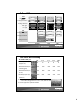
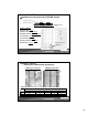
Focus Packages - Bumping, WLCSP, FCBGA, SIP, SCSP and
modified LF package
Small & Light -
Thin Thickness
Thin Thickness in Wafer, Substrate, Package
-
Fine Pitch
Fine Pitch
in Wire Bonding, Flip Chip Bond and
Solder Ball
-
High Density
High Density
by Stacked Die, Package, Multi-
Substrate Layer,Substrate Stacked, Staggered Via
and Small Trace Via Hole Size
Good Thermal and Electrical Performance
-
High Speed and Low Thermal Resistance
High Speed and Low Thermal Resistance
-
Cu / Low
Cu / Low
-
-
K wafer
K wafer, Nano-technology
Green -
Green Solution
Green Solution
Low Cost & Fast Time-to-market
-
12
12
’’
’’
Wafer Capacity
Wafer Capacity
- Total Turnkey Solution
- Matrix design, Multi-die, package Design
-
LAB Design Support
LAB Design Support
Trends of Packaging Technologies
安捷倫科技高頻元件量測研討會
2/23/2006
Page 10
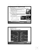
Outline
Development Trend for PKG
-- PKG Technology Trend
-- Why SiP and POP/PIP
Challenges to PKG Integrity Design
-- Design Challenges on Simulation, Measurement and Design
-- Case I : Effective DK
-- Case II : Impedance Control verify by TDR
-- Case III: TDR FA Application
-- Case IV : Substrate Ball Pad Design
-- Case V : PDS Analysis
Integrated Design
-- Components of Optimization PKG Design
-- Advanced PKG Analysis Flow
-- Plan and Actions for PKG Design