HV-FX5100 K SERVICE MANUAL VIDEO CASSETTE RECORDER BASIC TAPE MECHANISM : OVD-6 SPECIFICATIONS OPERATING TEMPERATURE ........... VIDEO RECORDING SYSTEM .......... VIDEO SIGNAL SYSTEM ................... VIDEO HEAD ...................................... USABLE CASSETTES ........................ CHANNEL COVERAGE ...................... RF OUTPUT ........................................ HORIZONTAL RESOLUTION ............ TIMER BACKUP ................................. TUNER SYSTEM ...........................
TABLE OF CONTENTS SPECIFICATIONS .............................................................................................................................................................. TABLE OF CONTENTS ..................................................................................................................................................... SERVICING NOTICES ON CHECKING ..........................................................................................................................
SERVICING NOTICES ON CHECKING 1. KEEP THE NOTICES 3. PUT PARTS AND WIRES IN THE ORIGINAL POSITION AFTER ASSEMBLING OR WIRING As for the places which need special attentions, they are indicated with the labels or seals on the cabinet, chassis and parts. Make sure to keep the indications and notices in the operation manual. There are parts which use the insulation material such as a tube or tape for safety, or which are assembled in the condition that these do not contact with the printed board.
DISASSEMBLY INSTRUCTIONS 1-3: DECK CHASSIS (Refer to Fig. 1-3) 1. REMOVAL OF MECHANICAL PARTS AND P.C. BOARDS 1-1: TOP CABINET, FRONT CABINET AND OPERATION 1, 2 PCB (Refer to Fig. 1-1) 1. Remove the 4 screws 1. 2. Remove the Top Cabinet in the direction of arrow (A). 3. Disconnect the following connectors: (CP651 and CP652). 4. Unlock the 7 supports 2. 5. Remove the Front Cabinet in the direction of arrow (B). 6. Remove the 3 screws 3 and remove the Operation 1 PCB. 7.
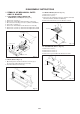
DISASSEMBLY INSTRUCTIONS 2. REMOVAL OF DECK PARTS NOTE 2-1: TOP BRACKET (Refer to Fig. 2-1) When you install the Tape Guide L, install as shown in the circle of Fig. 2-3-B. (Refer to Fig. 2-3-B) 1. Remove the 2 screws 1. 2. Slide the 2 supports 2 and remove the Top Bracket. NOTE Tape Guide L When you install the Top Bracket, install the screw (1) first, then install the screw (2). REC Lever (2) (1) 1 1 Top Bracket Top Bracket • The REC Lever is not installed on the Video Cassette Player. Fig.
DISASSEMBLY INSTRUCTIONS 2-6: LINK ASS'Y (Refer to Fig. 2-6) 2-9: TENSION ASS'Y (Refer to Fig. 2-9-A) 1. Set the Link Ass'y to the Eject position. 2. Remove the (A) side of the Link Ass'y first, then remove the (B) side. 1. Move the Inclined S Ass'y to the back side. 2. Unlock the support 1 and remove the S Reel Stopper. 3. Remove the Tension Spring. 4. Unlock the support 2 and remove the Tension Arm Ass'y. 5. Remove the Tension Adjust. 6. Unlock the 2 supports 3 and remove the Tension Band Ass'y. 7.
DISASSEMBLY INSTRUCTIONS 2-11: S REEL/T REEL ASS'Y (Refer to Fig. 2-11) NOTE 1. Remove the Idler Ass'y. 2. Remove the S Reel and T Reel Ass'y. 3. Remove the 2 Polyslider Washers 1. 1. Do not touch the Pinch Roller. (Use gloves.) 2. When you install the Pinch Roller Ass'y, install as shown in the circle. (Refer to Fig. 2-12-B) NOTE 1. Take care not to damage the gears of the S Reel, T Reel Ass'y and Idler Ass'y. 2. The Polyslider Washer may be remained on the back of the reel. 3.
DISASSEMBLY INSTRUCTIONS 2-15: AHC ASS'Y/CYLINDER UNIT ASS'Y (Refer to Fig. 2-15) 1 Middle Gear 1. Unlock the support 1 and remove the AHC Ass'y. 2. Remove the 3 screws 2. 3. Remove the Cylinder Unit Ass'y. E-Ring Main Cam 2 NOTE Pinch Roller Cam When you install the Cylinder Unit Ass'y, tighten the screws from (1) to (3) in order while pulling the Ass'y toward the left front direction. 3 Joint Gear Link Lever Spacer P5 Cam 2 (3) AHC Ass'y Fig.
DISASSEMBLY INSTRUCTIONS 2-19: LOADING GEAR S/T ASS'Y (Refer to Fig. 2-19-A) 2-20: INCLINED S/T ASS'Y (Refer to Fig. 2-20) 1. Remove the E-Ring 1 and remove the Main Loading Gear. 2. Remove the Capstan Brake Spring. 3. Slide the Main Rod and remove the Capstan Brake Arm Ass'y. 4. Remove the Main Rod. 5. Remove the Tension Lever. 6. Unlock the 2 supports 2 and remove the Clutch Lever. 7. Remove the screw 3 and washer 4. 8. Remove the LED Reflecter. 9. Remove the Loading Arm S Ass'y and Loading Arm T Ass'y.
KEY TO ABBREVIATIONS A A/C ACC AE AFC AFT AFT DET AGC AMP ANT A.PB APC ASS'Y AT AUTO A/V B BGP BOT BPF BRAKE SOL BUFF B/W C C CASE CAP CARR CH CLK CLOCK (SY-SE) COMB CONV CPM CTL CYL CYL-M CYL SENS D DATA (SY-CE) dB DC DD Unit DEMOD DET DEV E E EF EMPH ENC ENV EOT EQ EXT F F FBC FE FF FG FL SW FM FSC FWD G GEN GND H H.P.
KEY TO ABBREVIATIONS S SYNC SYNC SEP T TR TRAC TRICK PB TP U UNREG V V VCO VIF VP V.PB VR V.
SERVICE MODE LIST This unit provided with the following SERVICE MODES so you can repair, examine and adjust easily. Method Press both PLAY button and CH UP button on the set for more than 2 seconds. Press both FF button and CH UP button on the set for more than 2 seconds. Operations Initialization of the factory. NOTE: Do not use this for the normal servicing. PLAY/REC total hours are displayed on the FIP. Refer to the "PREVENTIVE CHECKS AND SERVICE INTERVALS" (CONFIRMATION OF USING HOURS).
PREVENTIVE CHECKS AND SERVICE INTERVALS The following standard table depends on environmental conditions and usage. Unless maintenance is properly carried out, the following service intervals may be quite shortened as harmful effects may be had on other parts. Also, long term storage or misuse may cause transformation and aging of rubber parts. Time Parts Name 500 hours 1,000 hours 1,500 hours 2,000 hours 3,000 hours Notes Audio Control Head Clean those parts in contact with the tape.
PREVENTIVE CHECKS AND SERVICE INTERVALS CLEANING NOTE 2. TAPE RUNNING SYSTEM After cleaning the heads with isopropyl alcohol, do not run a tape until the heads dry completely. If the heads are not completely dry and alcohol gets on the tape, damage may occur. When cleaning the tape transport system, use the gauze moistened with isopropyl alcohol. 3. CYLINDER Wrap a piece of chamois around your finger. Dip it in isopropyl alcohol. Hold it to the cylinder head softly.
NOTE FOR THE REPLACING OF MEMORY IC If a service repair is undertaken where it has been required to change the MEMORY IC, the following steps should be taken to ensure correct data settings while making reference to TABLE 1.
SERVICING FIXTURES AND TOOLS (For 1 speed model) VHS Alignment Tape JG001E (TTV-P2) JG001F (TTV-P1L) JG001U (VP 1 S-X6 3 ) (For 2 speed model) VHS Alignment Tape JG001C (TTV-P2) JG001D (TTV-P1L) JG001V (VP 2 S-X6 3 ) JG002B Adapter JG002E Dial Torque Gauge (10~90gf•cm) JG002F (60~600gf•cm) JG005 Post Adjustment Screwdriver Part No. SV-TG0-030-000 (small) JG153 X Value Adjustment Screwdriver JG022 Master Plane JG024A Reel Disk Height Adjustment Jig JG100A Torque Tape (VHT-063) JG154 Cable Parts No.
VCR TEST TAPE INTERCHANGEABILITY TABLE There are two types of the new alignment tape CH-1B (for NTSC) and CH-2 (for PAL). On each tape four signals (1) - (4) are recorded for the times and in the order shown below. (1) : 8min. ---> (2) : 2min. ---> (3) : 5min. ---> (4) : 5min. The TTV-MP1 (for M-PAL), TTV-MS1 (for MESECAM) and TTV-S1 (for SECAM) alignment tapes have the same contents as the previous tapes.
MECHANICAL ADJUSTMENTS 1-2: CONFIRMATION AND ADJUSTMENT OF TENSION POST POSITION 1. CONFIRMATION AND ADJUSTMENT Read the following NOTES before starting work. 1. Set to the PLAY mode. 2. Adjust the Tension Adjust until the length from the edge of the Tension Arm to the standard line of the Main Chassis is 0.5 ± 0.25mm. After this adjustment, confirm that the cut position is located in "A" area as shown in Fig. 1-2-B. If it is located in "B" area, adjust again. 3.
MECHANICAL ADJUSTMENTS 1-4: CONFIRMATION OF VSR TORQUE 1. Operate within 4~5 seconds after the reel disk begins to turn. 2. Install the Torque Gauge (JG002F) and Adapter (JG002B) on the S Reel. Set to the Rewind mode. (Refer to Fig.1-4) 3. Then, confirm that it indicates 120~180gf•cm. 2. CONFIRMATION AND ADJUSTMENT OF TAPE RUNNING MECHANISM NOTE Tape Running Mechanism is adjusted precisely at the factory. Adjustment is not necessary as usual.
MECHANICAL ADJUSTMENTS 2-2: CONFIRMATION AND ADJUSTMENT OF AUDIO/ CONTROL HEAD 2-3: TAPE RUNNING ADJUSTMENT (X VALUE ADJUSTMENT) When the Tape Running Mechanism does not work well, adjust the following items. 1. Confirm and adjust the height of the Reel Disk. (Refer to item 1-1) 2. Confirm and adjust the position of the Tension Post. (Refer to item 1-2) 3. Adjust the Guide Roller. (Refer to item 2-1) 4. Confirm and adjust the Audio/Control Head. (Refer to item 2-2) 5.
MECHANICAL ADJUSTMENTS 3. MECHANISM ADJUSTMENT PARTS LOCATION GUIDE 5 6 4 3 7 2 1 8 12 11 10 9 1. Tension Adjust 7. P4 Post 2. Tension Arm 8. T Brake Spring 3. Guide Roller 9. T Reel Ass'y 4. P1 Post 10. Idler Ass'y 5. Audio/Control Head 11. S-S Brake Spring 6. X value adjustment driver hole 12.
ELECTRICAL ADJUSTMENTS Read and perform this adjustment when repairing the circuits or replacing electrical parts or PCB assemblies. 1. BASIC ADJUSTMENT CAUTION When replacing IC's or transistors, use only specified silicon grease (YG6260M). (To prevent the damage to IC's and transistors.) 1-1: PG SHIFTER CONDITIONS MODE-PLAYBACK Input Signal-Alignment Tape (JG001C) INSTRUCTIONS 1. Connect CH-1 on the oscilloscope to TP4001 and CH-2 to pin 19 of J4501. 2. Playback the alignment tape. (JG001C) 3.
ELECTRICAL ADJUSTMENTS 2.
TROUBLESHOOTING GUIDE POWER DOES NOT TURN ON Does DISPLAY light ? No Yes Is F501 broken ? Yes Replace F501. No Is the voltage at collector of Q507 about 5.6V ? Yes Check IC1002. No Check the peripheral circuit to pin 14 of T501. Is the voltage at pin 20 of IC1002 about 5V ? No Check IC1002. Yes Is the voltage at base of Q502 about 5V ? No Replace Q510. Yes Replace Q502.
TROUBLESHOOTING GUIDE POWER SHUTS OFF Insert a cassette and press PLAY button. Does it Power off in about 3 seconds ? Yes Check TAPE LOADING, LOADING BELT, DD MOTOR and CYLINDER MOTOR. Yes Check REEL SENSOR and BELT CAPSTAN. No Does it Power off in about 6 seconds ? No Check POWER BLOCK.
TROUBLESHOOTING GUIDE CYLINDER NOT ROTATING DURING PLAYBACK AND RECORDING Is the voltage at pin 2 of CP1002 about DC11.25V ? No Check AT 12.6V line of POWER BLOCK. Yes In playback, is the voltage at pin 5 of CP1002 about DC1.52V ? No Check IC1002. Yes Replace CYLINDER MOTOR.
TROUBLESHOOTING GUIDE AUDIO SHAKES Yes Replace AUDIO HEAD. Is AUDIO HEAD scratched ? No Is input level at pin 85 of IC1002 about 0.4Vp-p ? No Replace CAPSTAN DD UNIT. Yes In playback, is the voltage at pin 4 of CP1003 2.6V ? No Check IC1002. Yes Check AUDIO BLOCK.
TROUBLESHOOTING GUIDE CASSETTE TAPE IS NOT ACCEPTED Does WORM GEAR on CASSETTE LOADING BLOCK activate ? No Check FRONT LOADING GEARS and LOCKER. No Check LED and PHOTO SENSOR on SYSCON PCB. Yes When a cassette is inserted, is the voltage at pin 4 of IC1002 0V ? Yes When a cassette is inserted, Yes is the voltage between pins 3 and 4 of CP1004 about 9.8V ? Replace LOADING MOTOR. No When a cassette is inserted, is the voltage at pin 47 of IC1002 5V ? No Replace IC1002.
TROUBLESHOOTING GUIDE WHEN INSERTING CASSETTE, IT EJECTS IMMEDIATELY Does another cassette go down ? Yes Defective CASSETTE or CASSETTE LOADING BLOCK. No Check FRONT LOADING GEARS. No When cassette is inserted, is the voltage at pins 4 and 3 of IC1002 0V ? Yes Check IC1002.
TROUBLESHOOTING GUIDE FF/REW DO NOT WORK Is the voltage changing at pin 11 of IC1002 when you press FF/REW ? No Check pins 9 and 10 of IC1002 lines. Yes Check DECK MECHANISM.
TROUBLESHOOTING GUIDE TAPE LOADING IS OK, BUT UNLOADS IMMEDIATELY Does CYLINDER rotate ? No Is the voltage at pin 2 of CP1002 AT 12.6V ? Yes Yes In playback, is the voltage at pin 5 of CP1002 1.54V ? Yes Replace CYLINDER UNIT. No Does TP4001 feed HEAD SWITCHING PULSE signal ? Yes Check REEL SENSOR. No No Does PG PULSE signal appear at pin 86 of IC1002? Yes Replace IC1002. E-8 No Check Power circuit.
TROUBLESHOOTING GUIDE PLAYBACK PICTURE JITTERS HORIZONTALLY Is FG output level at pin 3 of CP1002 about 4.0Vp-p? No Replace CYLINDER MOTOR. Yes Is the voltage at pin 5 of CP1002 1.5V ? No Replace IC1002. Yes Replace CYLINDER MOTOR. PLAYBACK PICTURE SHAKES Is FG output level at pin 3 of CP1002 about 4.0Vp-p? No Replace CYLINDER MOTOR. Yes Is the voltage at pin 5 of CP1002 1.5V? No Replace IC1002. Yes Replace CYLINDER MOTOR.
TROUBLESHOOTING GUIDE AUTO TRACKING DOES NOT OPERATE By manual tracking, does the DC level at pin 84 of IC4001 change ? No Check CYLINDER UNIT. Yes In auto tracking, is the voltage at pin 6 of IC1002 more than DC 1V ? Yes No Does the CTL PULSE (about 4.6Vp-p) appear at pin 97 of IC1002? Yes Replace IC1002. E-10 No Check CONTROL HEAD.
TROUBLESHOOTING GUIDE WHEN IN PLAYBACK, FAST FORWARD OR REWIND MODE IS ACTIVATED, UNIT STOPS IMMEDIATELY Does CAPSTAN DD MOTOR rotate ? No Refer to section "CAPSTAN DD MOTOR NOT ROTATING". Yes Does the REEL SENSOR PULSE signal appear at pins 79 and 80 IC1002 ? No Check Q1001 and Q1002. Yes Replace IC1002.
TROUBLESHOOTING GUIDE PLAYBACK PICTURE JITTERS VERTICALLY No Does tracking noise appear in the picture ? Yes By adjusting the manual tracking UP/DOWN buttons, will the noise disappear in the picture ? No Check P/B ENVELOPE. Yes Are GUIDE POSTS the right height ? No Adjust GUIDE POST height. Yes Is PG SHIFTER adjustment 6.5H ? No Adjust PG SHIFTER. Yes Yes Replace IC1002. Is PB-Y waveform normal ? No Check PB-Y circuit.
TROUBLESHOOTING GUIDE NO PLAYBACK PICTURE Is E-E appearing on the Monitor TV ? No Is the voltage at pins12, 36, 61 and 90, 96 of IC4001 5V ? No Check Power circuit. Yes Yes Check VIDEO OUT LINE and IC4001. Is there FM signal at pins 78 and 79 of IC4001 ? No Check connection of the CYLINDER. Yes Is there VIDEO signal at pin 52 of IC4001 ? No Replace IC4001.
TROUBLESHOOTING GUIDE NO COLOR DURING PLAYBACK Does COMPOSITE signal appear at pin 52 of IC4001? No Replace IC4001. Yes Check Q4802 circuit.
TROUBLESHOOTING GUIDE PLAYBACK PICTURE IS NOISY (EVEN AFTER CLEANING HEADS) Is FM signal at pin 79 of IC4001 270mVp-p ? No Check CYLINDER UNIT. Yes Is FM signal at pin6 of IC1002 more than 1V ? No Perform the interchangeable adjustment of DECK. Yes Is VIDEO output at the emitter of Q4802 2Vp-p, and are there any noises ? No Check IC4001 and Q4802. Yes Replace J4501.
TROUBLESHOOTING GUIDE NO COLOR DURING SELF RECORDING AND PLAYBACK Does VIDEO signal appear at pin 31 of IC4001 ? No Replace J4501. Check VIDEO input circuit. Yes Does color signal at pin 52 of IC4001 ? No Check IC4001. Yes Check Q4802 EMITTER.
TROUBLESHOOTING GUIDE NO NORMAL AUDIO ON PLAYBACK Does audio appear on E-E ? No Refer to section "NO E-E". Yes Does AUDIO signal appear at No pin 2 of IC4001 6mVp-p ? Check C4039 and peripheral circuit. Yes Does AUDIO signal appear at pin 11 of IC4001 1Vp-p ? No Replace IC4001. Yes Check AUDIO HEAD for debris or stains. Check the connector from AUDIO HEAD is fully inserted into CP4002. Replace IC4001.
TROUBLESHOOTING GUIDE CAPSTAN DD MOTOR NOT ROTATING In playback is the voltage at pin 5 of CP1003 12V ? No Check POWER circuit. Yes Is the voltage at pin 8 of CP1003 5V ? No Yes In playback, check the voltage at pin 3 of CP1003 is 2V or at pin 62 of IC1002 is 2.5V ? No Replace IC1002. Yes In playback, is the voltage at pin 4 of CP1003 2.5V ? No Check pins 77, 78 of IC1002 and peripheral circuit. Yes Replace IC1002. Does DD MOTOR rotate now? If not, replace DD MOTOR.
TROUBLESHOOTING GUIDE AUDIO CAN NOT BE RECORDED Is BIAS level O.K at L4005 ? No Is the voltage at pin 2 of L4005 5.8V ? No Check POWER circuit. Yes Yes Is the voltage at pin 29 of IC1002 about 5V ? No Replace IC1002. Yes L4005 is broken or shorted. Is there AUDIO signal at pin 5 of CP4002 ? No Check the circuit between pin4 of IC4001 to pin 5 of CP4002. Yes Is there AUDIO signal at pin 11 of IC4001 ? No Replace IC4001. Yes Check the lead wire and connector to A/C HEAD.
TROUBLESHOOTING GUIDE CASSETTE IN AND DOWN, UNIT HAS NO FUNCTIONS Does mode indicator appear in Display ? No Check LOADING MOTOR and the peripheral parts. Yes Does VCR operate with the remote control ? No Check IC1002. Yes Check Operation PCB.
TROUBLESHOOTING GUIDE RECORDING MECHANISM WORKS,BUT NO VIDEO RECORDED FROM INPUT JACK OR TUNER Does VIDEO signal appear at pin 31 of IC4001 ? Check the circuit from VIDEO input jack to IC4001, from Tuner Pack to IC4001. No Yes No Does the VIDEO signal appear at pin 52 of IC4001 ? Replace IC4001. Yes Check CYLINDER UNIT .
TROUBLESHOOTING GUIDE NO E-E(VIDEO AND AUDIO FROM TUNER) Are the plugs connected to the VIDEO/AUDIO input jacks ? Disconnect the plugs from the VIDEO/AUDIO input jacks. Yes No Do the voltages appear at each terminal PB(5V), TU(32V) and B+(5V) of TU6001 ? No Check Power Block. Yes CHECK AUDIO Does AUDIO signal appear at pin 21 of TU6001 ? Yes Does AUDIO signal appear at pin 1 and 2 of IC6601 ? Yes Check IC5501. CHECK VIDEO No No Replace TU6001.
TROUBLESHOOTING GUIDE NO E-E AUDIO (MONO) Is the voltage at pin 40 of IC5501 5V ? No Check POWER BLOCK. Yes Is the voltage at pin 34 of IC5501 12V ? No Check POWER BLOCK. Yes Does AUDIO signal appear at pins 6 and 7 of IC5501 ? No Check J4501 and peripheral circuit. Yes Does AUDIO signal appear at pin 21 of IC5501 ? No Replace IC5501. Yes Does AUDIO signal appear at pin 22 of IC5501 ? No Check IC4001. Yes Does AUDIO signal appear at pins 15 and 18 of IC5501 ? No Replace IC5501.
TROUBLESHOOTING GUIDE NO E-E AUDIO (STEREO) Does audio appear on E-E ? No Refer to section " NO E-E AUDIO (MONO) ". Yes Check the circuit between IC5501 to J4501.
TROUBLESHOOTING GUIDE NO TUNER AUDIO (MONO) Does audio appear on E-E ? No Refer to section " NO E-E AUDIO (MONO) ". Yes Does AUDIO signal appear at pin 38 of IC6601 ? No Check pin 21TU6001. Yes Does AUDIO signal appear at pins 1 and 2 of IC6601 ? No Replace IC6601. Yes Does AUDIO signal appear at pins 15 and 18 of IC5501 ? No Replace IC5501. Yes Check J4501 and peripheral circuit.
TROUBLESHOOTING GUIDE NO TUNER AUDIO (STEREO) Does signal appear at pin 25 of IC6601 ? No Reploce TU6001. Yes Refer to section "NO TUNER AUDIO (MONO)".
TROUBLESHOOTING GUIDE NO PB AUDIO (Hi-Fi) Does audio appear on E-E ? No Refer to section " NO E-E AUDIO (STEREO) ". No Refer to section " NO NORMAL AUDIO ON PLAYBACK ". Yes Does audio appear on PB ? Yes Is the voltage at pin 44 of IC5501 high ? No Replace IC1002. Yes Replace IC5501.
TROUBLESHOOTING GUIDE Hi-Fi AUDIO CANNOT BE RECORDED Does audio appear on E-E ? No Refer to section " NO E-E AUDIO (MONO) ". Yes Is the voltage at pin 44 of IC5501 hight ? No Replace IC1002. Yes Replace IC5501.
IC DESCRIPTIONS OEC7035A Pin No. Pin Name I/O Description 1 AFT-SC I AFT S Curve input for tuner. 2 AGC-DET I Input of CASS DOWN, TAB switch and setting of service mode. 3 EOT I Tape end sensor input signal. 4 BOT I Tape start sensor input signal. 5 RF SW/A-ENV I Ground. 6 V-ENV I Input terminal of video RF envelope. 7 KEY-A I Key A input. 8 KEY-B I Key B input. 9 MSSW A O Input terminal (A) of mecha state sensor. 10 MSSW B O Input terminal (B) of mecha state sensor.
IC DESCRIPTIONS OEC7035A Pin No. Pin Name I/O Description 51 POWER ON L O For control the user power switch ON/OFF. 52 NC O Not used. 53 ONE TOUCH PB O Control the LED for the ONE TOUCH PLAYBACK. 54 PELI CTL I Control the 21 pin IC output. 55 NC O Not used. 56 NC O Not used. 57 A.MUTE-H O This pin output the HIGH to mute the sound at the switching point between E-E and V-V during the special playback. 58 T.A.MUTE-H O Not used. 59 TAB SW I Input of TAB SW. 60 NC I Not used. 61 SD O Not used.
SERVO TIMING CHART IC1001 (OEC7035A) DPG *6 PIN DFG *7 PIN H. SW.
SYSTEM SWITCH MODE PB FWD : CAPSTAN FWD ROTATING DIRECTION RVS : CAPSTAN RVS ROTATING DIRECTION LOADING DIRECTION (FWD) EJECTION UNLOADING SLOW : SETTING SPEED TO SERVO : MECHANICAL MOVEMENT AND CAPSTAN ROTATING : MECHANICAL MOVEMENT (NO CAPSTAN ROTATING) STP3 VSR F.
SEMICONDUCTOR BASE CONNECTIONS DIODE CATHODE ANODE 11DF2N-TA2B2 1SS133T-77 GMA-02-BT MTZJ12B T-77 MTZJ15B T-77 MTZJ27B T-77 MTZJ33B T-77 MTZJ4.
Y/C/AUDIO/HEAD AMP BLOCK DIAGRAM X4001 4.433619MHz 79 75 78 58 60 73 55 52 54 CYL 1 EP/LP-CH2(L) 91 2 EP/LP COM 92 3 EP/LP-CH1(R) 93 4 SP-CH2(L) 94 5 SP-COM 86 6 SP-CH1(R) 87 7 HF2(L) 88 8 FH COM 89 9 HF1(R) 2MLPF CTL TRAP fh HPF ACC R P TRAP 6db AMP DELAY CLPF CLPF R P IIC DATA 63 V.H_SW ENV.DET 81 84 Q4005 Q4006 Q4007 AE HEAD(-) 6 AUDIO PB MIX LEVELADJ ENV DET R R N P CLEAR SYNC P B.
SYSTEM CONTROL/SERVO/TIMER BLOCK DIAGRAM LOADING MOTOR DRIVER IC1001 BA6955AN SYSCON/SERVO/TIMER IC1002 OEC7035A 2 28 HEATER SW HEATER SW 82 P.FAIL POWER FAIL POWER 27 CAP HI-H CAP HI-H 5 7 4 IC1004 RE5VS31A P.CON 5V SYSTEM RESET 1 REEL SENSOR Q1002 X1002 32.768KHz 2 LDM - 3 LDM + 4 A.ENV KEY-A KEY-A 7 OPERATION CH.
TUNER/HIFI/21PIN/OSD/VPS/NICAM BLOCK DIAGRAM HIFI IC5501 TDA9605H RECORD LUMINANCE SIGNAL PLAYBACK LUMINANCE SIGNAL RECORD COLOR SIGNAL PLAYBACK COLOR SIGNAL TUNER VIDEO SIGNAL AUDIO SIGNAL (REC) AUDIO SIGNAL (PB) PPL 1.3M/1.4M CCO BPF 1.3M/1.4M 35 LPF NOISE REDUCTION J4204 2 HF LPF 37 BPF 1.7M/1.8M 36 3 J4501 3 PPL 1.7M/1.
OPERATION BLOCK DIAGRAM V651 7-MT-201G 23 17 14 4 26 25 2 1 HEATER_DC + HEATER_DC - CH.UP IC651 BU2979K 14 17 19 21 41 CH.UP_SW 31 Q601 POWER OTPB SW STILL/PAUSE FIP DRIVER POWER OTPB OTP D601 SYSCON/ SERVO/TIMER OS651 CH.DOWN REMOCON 1 STOP/EJECT KEY-A REC/OTR FF/CUE PLAY REW/REV POWER BLOCK DIAGRAM D525 CAP VCO Q508 IC502 NJM431L Q509 CAP HI-H CAP SW CAP VCO SW VOLTAGE CTL. 1 AT +5.8V 2 Q512 Q501 PHOTO COUPLER SW REG IC501 STR-F6552 P.ON 5V SW P.
A B C D E F G H DECK SCHEMATIC DIAGRAM 8 8 LOADING MOTOR M101 7 7 (DECK PCB) S105 6 6 5.1 0 BOT SENSOR Q101 RPT-38PB113 S106 S101 S102 S103 S104 5 5 FROM/TO SYSCON/SERVO/TIMER CP101(CP1004) 52044-0445 LDM+ 1 2 LDM- 3 BOT 4 VCC FROM/TO SYSCON/SERVO/TIMER CP102(CP1001) 173979-2 4 2 1 VCC EOT 4 5.
A B C D E F G H OPERATION SCHEMATIC DIAGRAM 8 8 7 7 (OPERATION 2 PCB) (OPERATION 1 PCB) 6 OTPB SW Q601 DTA143ES 0 5.1 220 5.1 R607 6 CH25082A 1 OTPB R609 3.3K 2.7K SKQNAED010 R608 OTPB SW610 CH.DOWN SW607 470P B SKQNAED010 KEY-A POWER SW609 5 5 C601 SKQNAED010 GND SKQNAED010 AT+5V 4 SKQNAED010 STILL/PAUSE SW606 CH.UP_SW 3 CH.UP SW608 2 R606 1.
PRINTED CIRCUIT BOARDS SW606 OPERATION 1 DECK OPERATION 2 CP101 SW603 CP102 CD601 SW602 SW608 R603 R605 SW607 Q101 R607 R609 R608 D601 SW605 R602 R601 R604 SW604 SW601 C601 R606 CD602 Q601 SW609 SW610 J-3 Q102
R661 R543 Q503 Q651 C653 C654 J-4 23 34 Q502 1 R1027 R1022 12 R653 R654 Q4801 23 34 R1063 R4808 C6606 C6608 C6607C6611 R4802 R4816 D6601 12 Q4802 C4822 IC4801_1 C4809 R6606 C6614 R6607 R6611 C6619 C6620 R6614 R6609 C6621 R6014 R6011 R6016 C6021 C4058 R4814 R1065 R4501 R5503 R5504 C6011 R4522 C4504 C4510 C4505 C4507 C4502 C4501 C4511 C4541 C4525 C4516 R4502 C6612 Q4501 R1009 C4517 R5510 R5512 IC4501 IC 66 01 23 C4523 R4813 C4814 C4816 R1058 C5521 R4514 R55
W036 W100 OS651 W115 R537 W206 W211 C651 W046 W045 R1043 W009 W184 W271 W156 W037 R544 C660 C659 W098 W101 W005 V651 IC1099 Q505 Q507 C534 W154 W099 C531 R529 W210 C4808 L4806 SW1001 R538 D521 D527 C524 R525 W141 W142 W143 W144 R1038 X1002 C1022 W842 W832 L501 C1028 C533 R528 W209 CP651_1 W153 R1012 Q512 D1006 R548 W152 R1005 C4812 R541 D532 C1010 W118 D1007 W010 L4802 W208 L4803 W275 W104 C4802 R533 W821 W805 D525 W818 C6610 W105 W243 C4817 W004 R1056
R661 CP651_1 W100 R662 W101 R658 C652 R657 C658 C656 IC 65 1 R651 R656 C651 C1017 R1041 L4806 C4819 C4818 SW1001 W046 W045 R1043 C4810 C4808 R4812 R525 C524 C1020 R1026 W099 R1038 W842 W275 W104 R4810 W832 C6610 W105 W243 C4802 C4803 C4801 R4804 W821 W805 W035 R1020 R1024 R1028 C519 W253 R1046 IC 10 02 W032 W820 R4814 W059 W240 W151 W179 R4803 L4805 R4815 C6612 R4528 W237 C6605 W863 W803 R6619 R6618 C6613 R6601 D6601 12 R6606 C6614 R6607 L6605 R6611
A B C D E F G H Y/C/AUDIO/HEAD AMP SCHEMATIC DIAGRAM CH FE HEAD(GND) 2 FE HEAD(HOT) CAUTION: DIGITAL TRANSISTOR 1 4.7K 0.7 C EE/VV_V_OUT DUMMY_V.SYNC 0.1 B 18P CH C4082 39uH 0.01 B 25 26 27 34 33 29 50V3.3 KA C4103 6.3V 47 KA 0.01 B 5.2 C4090 5.2 5 3.5 C4105_1 5.2 180P CH 0.1 5.2 L4015 3.3 100uH P.CON+5V 0 0 0 2.8 SWD_VIDEO_IN 4 30 R4051 0 2.7 1.7 2.8 10 0.1 B C4079 C4094 0.01 B 3.8 AGC 28 16V 10 KA 3.3K C4077 W890 W891 0.1 B R4053 0.1 B C4074 0.
67 69 70 71 72 0 5.0 5.0 5.0 5.0 3.0 3.0 77 78 0 0 0 1.9 2.5 1.8 6 A FG 7 CAP.M F/R 8 VCC(5V) AT+5V RGB_ON-H CG_DATA PERI_CTL-L CG_CLK 22K R1044 C1035 FF/REW SW Q1007 DTC124EKA 0 C1037 0.1 B 0.001 B C1027 2.6 IIC_CLK CTL+ CTL- C1036 2.6 50V4.7 KA 5 6.3V 47 KA 0 R1065 2.1 0.7 R1063 2.6 R1062 1K CYL_FG 1K 150PCH 0 4.2 FROM/TO NICAM CYL_PG C1042 1K R1064 50V 1 0.
D E F 47P CH 1K R4528 R4524 DEC_A_OUT-L L4501 R4504 22uH 560 6dB BUFFER Q4802 2SA1037AK PERI_A_OUT-R R4522 6 2.5 7 5.1 75 75 R4515 470P B R4514 C4524 C4520 470P B 10uH L4512 11 NC 14 13 39 38 16 15 41 40 42 18 17 20 19 21 5 NC 560 18 C4810 0 C4519 2 TV-L/VCR-[10V] 15 1 L4507 R4508 22uH 2.7K PERI_VIDEO_OUT 3 REAR AUDIO OUT J4204 JPJ1195-010320 E 3 C4503 R4507 75 16V 470 YK PERI_VIDEO_IN R4516 50V 4.7 KA 0.022 B C4809 6.3V 47 KA C4808 0.022 B 6.
A B C D E F G H TUNER/HIFI SCHEMATIC DIAGRAM AFT_S_CURVE AGC_DET IIC_DATA IIC_CLK HIFI_H.SW/VV-H HIFI_REC_MUTE HIFI_ENV.DET 8 FROM/TO SYSCON/SERVO/TIMER RF_CONV.V TU_V_OUT DEC_A_OUT-R DEC_A_OUT-L PERI_A_OUT-R PERI_A_OUT-L PERI_A_IN-R PERI_A_IN-L DEC_A_IN-R DEC_A_IN-L FROM/TO 21PIN/OSD/VPS HF_COM HF2 HF1 NORMAL_A_OUT NORMAL_A_IN FROM/TO Y/C/A/H.AMP GND GND AT+12V GND (HIFI) (TUNER) P.CON+5V-A (AUDIO) P.CON+5V FROM POWER +32V (SYSCON PCB) 8 25 C6013 6.
A B C D E F G H POWER SCHEMATIC DIAGRAM 8 8 (SYSCON PCB) D512 ECQ-UV 1N4005E D505 C523 25V 330 VR D519 L502_1 22uH ELC0607 P.ON SW Q502 DTC143EKA D531 5.6K 220 RS C527 1.2K 50V 2.2 KA 25V D521 AT+12.6V 11EQS04N 1K R538 4 D532 5.7 5.0 CAP_VCO D530 1N4005E AT+5.8V P.CON+5V 0 POWER_ON-H P.ON SW Q510 4.9 DTC143EKA 3 HEATER_DC-30V 0.01 F C533 0 5.1 0.01 F 5.0 100K GND C531 22K H.ON SW Q503 DTA124EKA HEATER_DC+ -18.1 R537 2 -18.8 6.3V 1000 YK R543 -18.
A B C D E F G H DISPLAY SCHEMATIC DIAGRAM (SYSCON PCB) 8 V651 8 7-MT-201GA 6G 7G OTR 5G 4G 3G h b col2 SLPM g col1 j c VCR ATR APM b h f k g e V651 (7-MT-201GA) ANODE CONNECTION 1G 2G a c j d 1 Vout 1 6G 5G 4G 3G 2G 1G S h h h h h M P2 L k P3 M col2 P4 -18.8 -18.8 2 -25.7 4 P1 -27.0 5 P2 -19.8 6 P3 -9 -12.7 P4 -12.7 7 P5 -20.4 -27.6 -16.8 P6 P7 P8 P9 P11 P10 -30 -20.4 -13.2 -24.0 -24.0 -24.0 -24.0 -24.0 -24.0 -24.
A B C D E F G H NICAM SCHEMATIC DIAGRAM 8 8 (SYSCON PCB) 7 7 FROM/TO SYSCON/SERVO/TIMER IIC_DATA R6619 100 IIC_CLK W834 0607 FROM POWER 6.3V 47 KA C6625 47P CH C6616 R6618 100 L6601 100uH P.CON+5V-A 6 6 47P CH 0.01 B 22 I REF 18 11 TP1 33 SCK TEST2 17 12 PCLK 34 SYSCLK 13 ADDR1 35 VDDD4 44 VSSA3 22 TEST1 P2 XTAL1 43 VDDA3 21 VDDA2 V TUNE TP2 VDDD2 VSSD2 7 8 0 9 0.1 B C6621 5 2.4 0 NC 2.9 3.6 C6620 C6619 22P CH 22P CH X6601 R6607 3.3 10K 0 5.
A B C D E F G H INTERCONNECTION DIAGRAM F/E HEAD 8 8 2 2 GND 22 5 6 FG 6 7 CAP.M F/R 7 8 VCC(5V) 8 25 26 28 30 31 32 35 GND 37 RED BLANKING GND 39 AUDIO PB 6 AUDIO PB 5 AUDIO REC 5 AUDIO REC 4 CTL+ 4 CTL+ 3 CTL- 3 AUDIO CONTROL CTL- 2 AE HEAD(-) 2 AE HEAD(-) 1 AE HEAD(+) 1 AE HEAD(+) GND 25 DEC.VIDEO OUT DEC.VIDEO IN A.IN GND 2 5 VCC 2 2 2 VCC EOT 1 1 1 EOT DECK PCB550 VE8851 EOT SENSOR Q102 MB 4 B+ SCL 5 RED GND V.
WAVEFORMS Y/C/AUDIO/HEAD AMP 1 REC 0.5V 10U/div 2 PB 200mV 10U/div 6 REC 10V 5U/div 11 REC, PB 0.5V 0.5V/div 7 REC, PB 200mV 0.5V/div 12 REC, PB 1V 5U/div SYSCON/SERVO/TIMER 3 POWER ON 100mV 50T/div 8 REC, PB 1V 5V/div 13 REC, PB 1V 5U/div 4 PB 100mV 5V/div 9 REC, PB 1V 0.5V/div 15 CASS. LESS 1V 10U/div 5 REC, PB 1V 5V/div 10 REC, PB 200mV 0.5V/div 17 REC, PB 1V 0.5s/div 18 REC, PB 1V 0.5s/div 16 CASS.
MECHANICAL EXPLODED VIEW 702 702 702 624 703 701 701 702 701 623 626 707 706 625 610 607 TU6001 603 704 603 704 602 608 PCB010 (SYSCON PCB ASS'Y) 708 634 609 705 612 629 616 PCB280 (OPERATION 2 PCB ASS'Y) 628 615 705 630 620 604 705 621 632 614 PCB270 (OPERATION 1 PCB ASS'Y) 618 617 606 633 627 619 611 613 621 622 605 631 601 L1-1
MECHANICAL REPLACEMENT PARTS LIST REF. NO. PART NO.
CHASSIS EXPLODED VIEW (TOP VIEW) 503 367 503 515 505 505 M2003 505 335 UN4001 319 507 313 334 370 318 508 AA H5001 502 H5002 355 314 349 321 501 506 348 305 328 356 309 336 310 347 313 512 301 370 304 508 A 512 361 303 329 AA 315 338 316 AA 317 AB AA 320 AA AB 359 353 M101 AA 502 366 A 357 371 368 BA 308 366 358 351 364 306 369 372 509 365 AA AA AA PCB550 (DECK PCB ASS'Y) 502 AA AA 363 AA 351 362 373 323 324 AA AA 511 352 360 CLASS PART NO.
CHASSIS EXPLODED VIEW (BOTTOM VIEW) 302 M2001 511 AA 340 AA 514 AA 341 AA 511 322 513 332 346 514 AA 342 346 331 311 AA 330 AA 333 345 339 350 AA 516 343 AA 344 503 510 AC 312 AA AA AB 307 354 326 AA 327 325 BA AA 512 AA 337 504 CLASS GREASE OIL PART NO. MARK G-555G AA G-488M AB FL-721 AC KYODO OIL SLIDAS No. 150 BA NOTE: Applying positions AA, AB, AC and BA for the grease or oil are displayed for this section.
CHASSIS REPLACEMENT PARTS LIST REF. NO. PART NO. 301 302 303 304 305 306 307 308 309 S5-OA5-000-220 S5-OP2-002-700 S5-OP9-006-890 S5-OP5-000-830 S5-OP8-003-240 S5-OA0-002-970 S5-OA2-000-810 S5-OA2-000-730 S5-OP6-005-530 310 311 312 313 314 315 316 317 318 319 DESCRIPTION Q'TY REF. NO. PART NO.
ELECTRICAL REPLACEMENT PARTS LIST REF.NO. PART NO. DESCRIPTION REF.NO. PART NO.
ELECTRICAL REPLACEMENT PARTS LIST REF.NO. PART NO. DESCRIPTION REF.NO. PART NO.
ELECTRICAL REPLACEMENT PARTS LIST REF.NO. PART NO. DESCRIPTION *** CRYSTAL & CERAMIC OSCILLATORS *** X1001 X1002 X4001 X6601 S0-0CT-012-070 S0-0D3-2R8-010 S0-0CF-4R4-010 S0-0CT-024-010 X'TAL,HC-49/U-S X'TAL,32.768K X'TAL,HC-49/U X'TAL,HC-49/U *** TUNER *** ! TU6001 S1-626-070-100 RF UNIT,TMDB2-103A *** FUSES *** ! F501 FH501 FH502 S8-0PT-1R6-020 S6-710-T00-060 S6-710-T00-060 FUSE,21801.
2–11, IKENOHATA 1–CHOME, TAITO-KU, TOKYO 110-8710, JAPAN TEL:03 (3827) 3111 920074 Printed in Singapore