NSX-AJ700 NSX-SZ700 NSX-SZ705 U LH LH SERVICE MANUAL COMPACT DISC STEREO SYSTEM BASIC TAPE MECHANISM : 2ZM-3MK2 PR9NM ZZM-3 PR1NM BASIC CD MECHANISM : BZG-5 ZD3N1M SYSTEM CD CASSEIVER TAPE MECHANISM SPEAKER NSX–AJ700 CX–NAJ700 ZZM-3 PR1NM SX–NAJ702 NSX–SZ700 CX–NSZ700 2ZM-3MK2 PR9NM SX–WNSZ703 NSX–SZ705 CX–NSZ705 2ZM-3MK2 PR9NM REMOTE CONTROLLER RC–BAS02 SX–NSZ705 • This Service Manual is the “Revision Publishing” and replaces “Simple Manual” NSX-AJ700 (U) / NSX-SZ700 (LH) / NSX-SZ705 (
SPECIFICATIONS Tuning range Usable sensitivity (IHF) Antenna terminals Tuning range Usable sensitivity Antenna Power output Total harmonic distortion Inputs Outputs 87.5 MHz to 108 MHz 13.2 dBf 75 ohms (unbalanced) 530 kHz to 1710 kHz (10 kHz step) 531 kHz to 1602 kHz (9 kHz step) 350 µV/m Loop antenna U : 100 W + 100 W (50 Hz to 20 kHz, T.H.D. less than 1 %, 6 ohms) 120 W + 120 W (1 kHz, T.H.D.
PROTECTION OF EYES FROM LASER BEAM DURING SERVICING This set employs laser. Therefore, be sure to follow carefully the instructions below when servicing. WARNING!! WHEN SERVICING, DO NOT APPROACH THE LASER EXIT WITH THE EYE TOO CLOSELY. IN CASE IT IS NECESSARY TO CONFIRM LASER BEAM EMISSION. BE SURE TO OBSERVE FROM A DISTANCE OF MORE THAN 30cm FROM THE SURFACE OF THE OBJECTIVE LENS ON THE OPTICAL PICK-UP BLOCK.
NOTE ON BEFORE STARTING REPAIR 1. Forced discharge of electrolytic capacitor of power supply block When repair is going to be attempted in the set that uses relay circuit in the power supply block, electric potential is kept charged across the electrolytic capacitors (C101, 102) even though AC power cord is removed. If repair is attempted in this condition, secondary defect can occur. In order to prevent the secondary trouble, perform the following measures before starting repair work.
In such a case, check also if the POWER AMPLIFIER circuit or power supply circuit has any abnormalities or not. 2-2. Regarding reset TE R There are cases that the machine does not work correctly because the MICROCOMPUTER is not reset even though the AC power cord is re-inserted, or the software reset (pressing the STOP key + POWER key) is performed. When the above described phenomenon occurs, it can lead to wrong judgement as if the MICROCOMPUTER is defective and to exchange the MICROCOMPUTER.
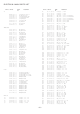
ELECTRICAL MAIN PARTS LIST REF. NO. PART NO. KANRI NO. REF. NO. PART NO.
REF. NO. PART NO. REF. NO. PART NO. KANRI DESCRIPTION NO. CAP, U 0.022-25 CAP,E 100-10 SMG CAP,E 0.47-50 SMG CAP,E 1-50 SMG CAP,E 1-50 SMG C404 C405 C406 C407 C408 87-012-193-080 87-012-286-080 87-012-286-080 87-012-286-080 87-012-286-080 KANRI DESCRIPTION NO. C-CAP,U 82P-50 CH CAP, U 0.01-25 CAP, U 0.01-25 CAP, U 0.01-25 CAP, U 0.
C173 C174 C180 C185 C186 87-010-421-040 87-010-421-040 87-010-759-080 87-010-759-080 87-012-274-080 KANRI DESCRIPTION NO. CAP,E 4.7-50 5L CAP,E 4.7-50 5L C-CAP,U, 0.1-25F C-CAP,U, 0.1-25F CHIP CAP,U 1000P-50B COIL,1UH K(MDEC) COIL,1UH K(MDEC) COIL,OSC 85K HZ BIAS COIL,FM DET-N(TOK) FLTR,PCFJZH-450 L(TOK) C188 C191 C192 C251 C315 87-012-369-080 87-012-286-080 87-010-759-080 87-A12-094-080 87-010-759-080 C-CAP,S 0.047-50F CAP, U 0.01-25 C-CAP,U, 0.1-25F CAP,E 47-50 SMG C-CAP,U, 0.
REF. NO. PART NO. ! ! ! ! T1 T2 T81 T82 WH81 87-A60-317-010 87-A60-317-010 87-A60-317-010 87-A60-317-010 87-A90-510-010 REF. NO. PART NO. KANRI DESCRIPTION NO. TERMINAL, 1P MSC TERMINAL, 1P MSC TERMINAL, 1P MSC TERMINAL, 1P MSC HLDR,WIRE 2.5-9P KANRI NO. DESCRIPTION BOX SW C.B S901 S902 87-036-252-010 87-036-252-010 SW,MICRO SPPB51 SW,MICRO SPPB51 DECK C.B M-OP-PANEL C.
TRANSISTOR ILLUSTRATION C B E E C B 2SA1235F 2SC2714O 2SC3052F KRA102S KRA107S KRC104S KRC107S CMBT5401 CMBT5551 RT1P141C B C E E C B 2SA1980G 2SA1981Y 2SA1979O/Y 2SC5343G 2SC5342Y CSD655E CC5551 CDA1585BC CSC4115BC KTA1266GR CSB1370EF S D G E C B D G S S D G 2SA933AS(R) 2SJ460 2SK2541 G D S B C E 2SK2937 FN1016 FP1016 2SK360E – 10 – 2SK2158
WIRING 1 (MAIN / PT) 32 31 30 29 28 27 26 25 24 23 22 21 20 19 18 17 16 15 14 13 12 11 10 9 8 7 6 5 4 3 2 1 A B C D E F G H I J K TO PT C.B CN001 (CNA001) TO PT C.
SCHEMATIC DIAGRAM _ 1 (MAIN 1 / 2 : AMP SECTION) – 12 –
SCHEMATIC DIAGRAM _ 2 (MAIN 2 / 2 : TUNER SECTION) – 13 –
SCHEMATIC DIAGRAM _ 3 (PT) – 14 –
WIRING 2 (FRONT / MOTOR / BOX SW ) 32 31 30 29 28 27 26 25 24 23 22 21 20 19 18 17 16 15 14 13 12 11 10 9 8 7 6 5 4 3 2 1 A , LED401 B C D E F G H TP8 I J K L M N O P Q S901 BOX 2 SW R S S902 BOX 1 SW T U 15
WIRING – 3 (M – OP – PANEL / S – OP – PANEL) 32 31 30 29 28 27 26 25 24 23 22 21 20 19 18 17 16 15 14 13 12 11 10 9 8 7 6 5 4 3 2 1 A B C D E F G H I J K L M N O P Q R S T U – 16 –
SCHEMATIC DIAGRAM _ 4 (U : FRONT / M-OP-PANEL / S-OP-PANEL / MOTOR / BOX SW / DECK ) – 17 –
SCHEMATIC DIAGRAM _ 5 (LH : FRONT / M-OP-PANEL / S-OP-PANEL / MOTOR / BOX SW / DECK ) – 18 –
WIRING 4 (PT) 14 13 12 11 10 9 8 7 6 5 4 3 2 1 A B C D E F G H I TO MAIN C.
SCHEMATIC DIAGRAM _ 6 (PT) – 20 –
WIRING 5 (LH : DECK / HEAD 1 / HEAD 2) 32 31 30 29 28 27 26 25 24 23 22 21 20 19 18 17 16 15 14 13 12 11 10 9 8 7 6 5 4 3 2 1 A B C D E F G H I J K L M N O P Q R S T U 21
WIRING 6 (U : DECK) 32 31 30 29 28 27 26 25 24 23 22 21 20 19 18 17 16 15 14 13 12 11 10 9 8 7 6 5 4 3 2 A TO FRONT C.B CN202 H DECK C.
FL (BJ815GNK) GRID ASSIGNMENT AND ANODE CONNECTION GRID ASSIGNMENT ANODE CONNECTION 23
IC BLOCK DIAGRAM 24
IC DESCRIPTION IC, LC866560W-5V01 Pin No. Pin Name I/O 1 O-C-SHIFT O Clock shift output for micro computer when tuner receiving broadcast. 2 O-POWER O Power control ON/OFF output. 3 O-2PB O DECK 2 / DECK 1 play output. 4 O-PANE-LED O Moving PANEL LED ON/OFF output (Not used). 5 O-DATA O Data output. 6 O-RMT O REC MUTE output. 7 O-BIAS O Bias ON/OFF output. 8 O-MUTE O System MUTE ON/OFF.
Pin No. Pin Name I/O Description 56 KARAOKE/P23 I/O Karaoke input to diode/FL segment P23 output. 57 DEMO/P22 I/O Demo (on the stop) diode input (Not used)/FL segment P22 output. 58 DOLBY/P21 I/O DECK DOLBYdiode input (Not used)/FL segment P21 output. 59 AM-ST/P20 I/O AM-ST select diode (Not used)/FL segment P20 output. 60 SOFT/P19 I/O DECK SOFT diode input (Not used)/FL segment P19 output. 61 SW/P18 I/O SW diode input (Not used)/FL segment P18 output.
Pin No. Pin Name I/O Description 97 O-CD CE O CD data chip enable output. 98 I-STEREO/I-DRF I Tuner stereo detect input/RF (radio frequency) detect. 99 O-P-DATA O Panorama IC data output (Not used). 100 O-CLK O PLL IC clock output.
ADJUSTMENT 3. PB Frequency Response Check (DECK 1, DECK 2) Settings : • Test tape : TTA–330 • Test point :TP5(Lch), TP6(Rch) Method : Play back the 315Hz and 8kHz signals of the test tape and check that the output ratio of the 10kHz signal with respect to that of the 315Hz signal is 0dB ± 5dB. < TUNER SECTION > 1. Clock Frequency Check Settings : • Test point : TP2 (CLK) Method : Set to AM 1710kHz and check that the test point is 2160kHz ± 45Hz. 2.
CD TEST MODE 1. How to Start the CD Test Mode While pressing the FUNCTION button, insert the AC plug to the power outlet. When the test mode is started, the message [CD TEST] is displayed. 2. How to Exit the CD Test Mode Press the POWER button or disconnect the AC plug. * When any key other than PLAY is pressed during play mode, the machine exits the test mode. 3.
MECHANICAL EXPLODED VIEW 1 / 1 BZG-5 A A A 46 54 45 A WIRE,BINDER PWB 59 A 60 G 44 42 47 F 43 FL401 11 12 a A 19 23 PWB 21 b A A 56 H H A 24 H H A PWB C 55 55 25 I 14 PWB 58 28 26 13 57 29 A B b 30 5 3 20 34 21 31 32 c 33 C 35 PLATE,PT 85 A 52 C PWB 51 B a c 14 36 1 22 17 NSZ700 LH NSZ705 LH 2 6 G 50 G 50 A A I A 7 E A 41 10 15 NAJ700 U 49 16 18 9 48 27 GUIDE,ECO 8 A HT-SINK, ASSY U E 4 40 A D 37 38 A PWB C A A CHAS,M
MECHANICAL PARTS LIST 1 / 1 REF. NO. PART NO. KANRI DESCRIPTION NO. WINDOW,CASS 1 WINDOW,CASS 2 BOX,CASS 1 1WAY BOX,CASS 1 REV BOX,CASS 2 1WAY REF. NO. PART NO. KANRI DESCRIPTION NO.
TAPE MECHANISM EXPLODED VIEW 1 / 1 TERMINAL, LB1 33 A 34 55 A 44 45 43 36 42 31 32 41 46 51 TERMINAL,LB1 33 45 51 35 A 52 44 52 31 32 b a 29 43 47 29 40 39 28 48 50 42 53 46 49 35 41 30 27 37 21 47 B 38 a 48 40 19 27 49 20 26 25 b 24 17 23 18 16 22 28 30 21 26 20 25 24 19 IC, EW732 23 18 22 IC, EW732 54 9 5 6 38 1 14 54 39 2 10 11 c c 5 6 3 37 9 14 15 16 PWB 10 7 11 12 8 4 12 15 13 – 32 – 13
TAPE MECHANISM PARTS LIST 1 / 1 31 32 33 34 35 8Z-ZM3-233-010 84-ZM2-227-310 87-A90-403-110 87-A90-404-010 8Z-ZM3-239-010 KANRI DESCRIPTION NO.
TAPE MECHANISM EXPLODED VIEW 1 / 1 A 44 B C 47 45 46 48 52 49 44 50 29 7 43 PWB.
TAPE MECHANISM PARTS LIST 1 / 1 REF. NO. PART NO. REF. NO. PART NO. KANRI DESCRIPTION NO. PULLEY,COUPLER M3 W-P,0.99-4-0.25 SLT BELT,MAIN L SPR-T,FR 60 GEAR,IDLER KANRI DESCRIPTION NO.
GENERAL SPEAKER DISASSEMBLY INSTRUCTIONS (FOR REFERENCE) Type.1 Type.4 TOOLS Insert a flat-bladed screwdriver into the position indicated by the arrows and remove the panel. Remove the screws of each speaker unit and then remove the speaker units. 1 Plastic head hammer 2 (() flat head screwdriver 3 Cut chisel 1 2 3 How to Remove the PANEL, FR Type.2 Remove the grill frame and four pieces of rubber caps by pulling out with a flat-bladed screwdriver.
SPEAKER PARTS LIST REF. NO. PART NO. 1 2 3 4 5 8B-NSJ-001-010 8B-NSJ-003-010 8B-NSJ-004-010 8B-NSJ-602-010 8B-NSJ-604-010 6 8B-NSJ-612-010 KANRI DESCRIPTION NO. PANEL,FR PANEL,DUCT PROTECTOR SPKR, W 160 SPKR, TW 60 CORD, SPKR SPEAKER PARTS LIST REF. NO. PART NO. 1 2 3 4 5 8B-NS8-001-010 8B-NS8-002-010 8B-NS8-003-010 8B-NS8-004-010 8B-NS8-007-010 6 7 8 9 8B-NS8-602-010 8B-NS8-604-010 88-NSK-610-010 88-NS5-610-010 KANRI DESCRIPTION NO.
2–11, IKENOHATA 1–CHOME, TAITO-KU, TOKYO 110, JAPAN TEL:03 (3827) 3111 2000058 0251431 Printed in Singapore