VX-F20DV1 U SERVICE MANUAL DVD COLOR TELEVISION BASIC DVD MECHANISM : AZG-D ZDADM • This Service Manual is the “Revision Publishing” and replaces “Simple Manual” (S/M Code No. 09-008-437-0T1). S/M Code No. 09-009-437-0R1 RE VI SIO DA N TA • If requiring information about DVD mechanism, see Service Manual of AZG-D, (S/M Code No.
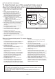
TABLE OF CONTENT SPECIFICATIONS ................................................................................................................................................................ 3 ACCESSORIES / PACKAGE LIST ...................................................................................................................................... 3 PROTECTION OF EYES FROM LASER BEAM DURING SERVICING ........................................................................ 4 NOTICES BEFORE REPAIRING .
SPECIFICATIONS TV SECTION Tuner System TV System Channel Coverage Program Memory Antenna Input Picture Tube Screen Size Video Input Audio Input Video output Audio output Digital Audio output Speaker GENERAL Frequency synthesized tuner NTSC-M VHF: 2 to 13 UHF: 14 to 69 CATV: 5A, A-1 to A-5, A to W, W+1 to W+84 181 75 ohms, unbalanced 20 in. 406 (W) x 305 (H) mm (16 x 121/8 in.) 508 mm (diagonal) (20 in.) 1 Vp-p, 75 ohms 0.5 Vrms., more than 33 k ohms 1 Vp-p, 75 ohms (sync negative) 0.5 Vrms., 2.
PROTECTION OF EYES FROM LASER BEAM DURING SERVICING This set employs laser. Therefore, be sure to follow carefully the CAUTION instructions below when servicing. Use of controls or adjustments or performance of procedures other than those specified herin may result in hazardous radiation exposure. WARNING!! WHEN SERVICING, DO NOT APPROACH THE LASER EXIT WITH THE EYE TOO CLOSELY. IN CASE IT IS NECESSARY TO CONFIRM LASER BEAM EMISSION.
NOTICES BEFORE REPAIRING To make the best use of this equipment, make sure to obey the following items when repairing (or mending). 1. Do not damage or melt the tunicate of the leading wire on the AC1 side, including the power supply cord. 2. Do not soil or stain the letters on the spec. inscription plates, notice labels, fuse labels, etc. 3. When repairing the part extracted from the conducted side of the board pattern, fix it firmly with applying bond to the pattern and the part. 4.
When repairing the Flat TV, never switch ON the main POWER with the degauss coil removed. If the degauss coil must inevitably removed due to some reason, connect a dummy using either Method 1 or Method 2 as described below. Method 1: Prepare a replacement degauss coil and connect it during repair. Method 2: Prepare a resistor of 2.8 ohm, 20 W. Manufacture a repair jig by connecting it to the degauss side connector. Connect the jig during repair.
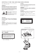
DISASSEMBLY INSTRUCTIONS 1. "CABINET" REMOVAL 1-1. Remove the 9 screws (A), 2 screws (B) and 4 screws (C) from the rear of of the set and remove the "Cabi, Rear". Cabi, Rear Fig-1 1-2. Remove 2 screws (D) and the screw (E) and remove the "Panel, Rear 2".
2. "TV. UNIT" REMOVAL 2-1. Anode cap disassembly 2-1-1. Notice Before Disassembly Discharge the anode. 1) Anode cap The cathode-ray tube of this equipment has the structure that the anode potential is automatically discharged when the power is off. But immediately after the POWER is turned off, there might be the case that the anode potential has not been discharged completely. When removing the Anode Cap, make sure to discharge the anode potential. Do not use a plier.
2-2. Anode cap assembly Make sure to keep the notices not to make troubles when assembling or disassembling the Anode Cap. Left Right 2-2-1. Notice Before Assembly Strictly forbidden to rotate Anode Cap after assembling. Anode Cap Do not use a deformed hook. If the Anode Cap is rotated after assembling, the Anode Cap may slip off. Route the high voltage cable before fixing the Anode Cap (See Fig-7).
4) Turn over the edge of the Anode Cap as the left figure (See Fig-10). Note) The right and left sides of the Anode Cap should be turned over equally. Note) Take enough care not to scratch the Anobe Cap. Fig-10 5) Hold the Anode Cap with the thumb and middle fingers while supporting the middle projection with the forefinger as the left figure. (See Fig-11-1) 6) Insert the one side of the hook to the anode button. (See Fig-11-2) Note) Confirm that the hook is surely hitched.
8) Pull it lightly while keeping the edge of the Anode Cap turned over. Visually confirm that the both hooks are inserted and check the condition of hitching of the shutter hook. 9) Remove hand from the rubber cap of the Anode Cap. Note) Put on the edge of the Anode Cap without clearance. Anode cap 10) Push the part of the skirt of the edge of the Anode Cap lightly and set the rubber cap and CRT to be adhered. 11) Furthermore, reconfirm that the Anode cap adheres closely to the CRT (See Fig-12).
2-3. Remove the connectors from the "TV, UNIT".
2-4. Remove the "NECK" board from the CRT. CRT PWB, NK Fig-17 2-5. Remove 2 screws (F) and pull out the "Frame, TV Assy" from the set.
3. HOW TO REMOVE "MAIN" BOARD AND "AUDIO" BOARD 3-1. Remove the connector that connects the "PWB, MAIN" and "PWB, AUDIO". CN701 CN706 CN705 CN702 CN409 CN707 Fig-19 3-2. Remove "PWB, AUDIO" and "PWB, MAIN" from "FRAME, TV".
4. HOW TO REMOVE "MECH, ASSY" BOARD 4-1. Remove the connector. CN110 CN216 Panel, Rear Assy CN107 Fig-21 4-2. Remove 2 screws (G) and the screw (H). Then pull out the "Mech, Assy" and "PWB, PS-SW" at the same time.
5. HOW TO REMOVE "PS-2" BOARD (WITH "PS-SW" BOARD), "JOINT" BOARD AND "AZG-D". 5-1. Remove 5 screws and remove the "Panel, Rear 1". Panel, Rear1 Fig-23 5-2. Remove 6 screws (J) and the connector. Then remove the "PWB, JOINT".
5-3. Remove 6 screws (K) and remove the "PWB, PS-2". PWB, PS-2 Fig-25 5-4. Remove 6 screws (L) and remove the "Shild, Assy".
5-5. Remove 4 screws (M) and 3 screw (N). Then remove the "Shld-Plate, Low". Shld-Plate, Low Fig-27 5-6. Remove 2 screws (O) and the screw (P). Then remove the "Hldr, Mech R Assy".
5-7. Remove 2 screws (Q) and the screw (R). Then remove the "Hldr, Mech L Assy". Hldr, Mech L Assy Fig-29 5-8. Remove the screw (S) and the connector. Then remove the "PWB, OPT". 5-9. Remove 2 screws (T) and remove the "Frame, Mech BK".
6. HOW TO REMOVE "FRONT" BOARD 6-1. Remove 15 screws (V) and remove the "PWB, SYSTEM" and "PWB, FR-JACK" . PWB, SYSTEM Fig-31 PWB, FR-JACK 6-2. Remove the connector and separate the 4 boards.
SERVICE POSITION When the AZG-D is going to be repaired, take the service position as follows. 1. Disassemble the set and take the AZG-D out. 2. Reassemble the set without installing the AZG-D. 3. Pull out 4 connectors that come from the AZG-D from the left side of the set and connect them. Note) Picture shows removal of the shield (SHLD-PLATE, LOW) from the bottom of the AZG-D.
WIRING ARRANGEMENT WIRE PROCESSING (WIRING, TYING) METHOD * * * Be sure to follow the instructions described as follows when processing the wires during disassembling and reassembling, in order to secure safety upon completion of the repair work. mark in the illustrations, are the parts that are specifically designed as the safety related The parts that are shown with the important parts by the safety regulations. Pay utmost care for these marks. For tying the wires, the following parts are mainly used.
2. Wiring in the periphery of the MAIN board. PWB, MAIN SAFETY CN707 CNA414 CN702 CN705 CN706 CNA403 CN409 CN405 CN401 CN402 CN701 PWB, AUDIO CAUTION: Must not touch to tuner (TU101). SAFETY CN771 CNA771 TU101 CN701 SAFETY HT801 To CN409 From CNA603 CAUTION: CNA603 GND wire must not touch to heat sink (HT801).
3. Wiring in the periphery of the left side of the CRT. 1cm SAFETY CN952 CN901 SAFETY CN903 SAFETY CN951 CNA704 SAFETY CN409 CN404 CNA408 4. Wiring in the periphery of the right side of the CRT. 14~16cm SAFETY DGC WIRE Around the twice. CN904 SAFETY CN901 CAUTION: DGC Wire must not touch to heat sink.
5. Wiring in the periphery of the PS-2 board.
6. Wiring of the AZG-D and JOINT board.
FF-Cable, 5p FF-Cable, 13p Mech, ASSY RED FF-Cable, 11p CN401 Core,Ferrite CN702 CN551 CN800 CLOTH TAPE PART NO. SV-T00-067-010 (Size:180mm x 90mm) 7. Wiring of the FRONT board.
ELECTRICAL MAIN PARTS LIST REF. NO. PART NO. KANRI NO. DESCRIPTION REF. NO. PART NO. KANRI NO. 87-070-092-080 87-A40-735-090 87-A40-001-080 87-017-593-090 87-017-654-060 DIODE,S5566B DIODE,ERC06-15 ZENER,MTZJ12C DIODE,RGP15J DIODE,GBU6J 87-A40-450-090 87-A40-828-080 87-A40-911-090 87-A40-734-010 87-A40-354-090 DIODE,RU 1P DIODE,AK 04 DIODE,RN 2Z DIODE,FML-G12S DIODE,UF3GL-6251 87-A40-337-080 87-A40-553-080 87-017-650-080 87-A40-503-080 87-070-173-010 ZENER,MTZJ 6.
REF. NO. PART NO. ! C211 C212 C213 C214 C229 KANRI NO. 87-A11-080-080 87-A11-080-080 87-A11-082-080 87-018-134-080 87-018-149-080 DESCRIPTION CAP,TC U 47P-50 J CH CAP,TC U 47P-50 J CH CAP,TC U 56P-50 J CH CAPACITOR,TC-U 0.01-16 CAP,TC-U 15P-50 CH C301 C302 C305 C306 C307 87-010-403-080 87-018-134-080 87-018-126-080 87-010-405-080 87-A10-299-080 C308 C309 C311 C312 C313 REF. NO. C626 C627 C629 C630 C631 KANRI NO.
REF. NO. PART NO. CNA803 D1 FB301 FB601 FB801 KANRI NO. 8A-JD1-669-010 87-070-110-010 87-003-320-080 87-003-223-080 87-003-320-080 CONN ASSY,2P TV TO PS LED,SLP-181B-51 RED F-BEAD,-9.
REF. NO. PART NO. C474 KANRI NO. 87-A10-295-080 DESCRIPTION CAP,M 0.01-50 J C475 C476 C477 C478 87-010-198-080 87-010-260-080 87-010-316-080 87-010-316-080 CAP, CHIP 1000P-50 KB CAP, ELECT 47-25V C-CAP,S 33P-50 CH C-CAP,S 33P-50 CH C479 C480 C481 C482 C483 87-010-318-080 87-010-316-080 87-010-316-080 87-010-196-080 87-010-260-080 C-CAP,S 47P-50 CH C-CAP,S 33P-50 CH C-CAP,S 33P-50 CH CHIP CAPACITOR,0.
REF. NO. PART NO. C106 C107 C108 C109 C110 KANRI NO. 87-010-405-080 87-010-405-080 87-010-405-080 87-010-405-080 87-012-286-080 DESCRIPTION CAP, CAP, CAP, CAP, CAP, ELECT 10-50V ELECT 10-50V ELECT 10-50V ELECT 10-50V U 0.01-25 C111 C112 C113 C114 C115 87-012-286-080 87-012-286-080 87-010-405-080 87-010-405-080 87-012-286-080 CAP, CAP, CAP, CAP, CAP, U 0.01-25 U 0.01-25 ELECT 10-50V ELECT 10-50V U 0.
REF. NO. PART NO. ! ! ! ! ! ! ! ! ! ! ! C242 C244 C245 CN211 CN216 KANRI NO. 87-012-370-010 87-A10-831-080 87-A10-374-010 87-A60-937-010 87-A60-632-010 DESCRIPTION CAP,CER 3300P-250NS CAP,E 1000-25 M SMG CAP,M/P 0.1-275 K RMR CONN,2P V VH CONN,15P V 2MM JMT CNA214 FB211 ICF211 ICF212 ICF213 8A-JD1-660-010 87-003-223-080 87-A91-337-080 87-001-132-080 87-A91-337-080 ICF214 ICF215 ICF216 L211 L212 REF. NO. C715 C716 CN701 CN702 CN703 KANRI NO.
CHIP RESISTOR PART CODE Chip Resistor Part Coding 8 8 A Figure Resistor Code Value of resistor Chip resistor L W t :A Resistor Code : A 1.0 0.5 0.35 104 1.6 0.8 0.45 108 2 1.25 0.45 118 3.2 1.6 0.
TRANSISTOR ILLUSTRATION C B E E C B 2SA1091-0 2SC1815GR 2SC2482 B C E B C E 2SC5147D 2SA1837 2SC4793 2SD2531 E C B B C E 2SA1015Y 2SD2578-CA B C E 2SC1741AS(R) E C B 2SA933SRS 2SA1175FE 2SC1740SRS 2SC2785FE B C E 2SB1237(Q) – 35 – 2SA1037K 2SC2412KR KRC104S DTA114EK DTC114EK KRA104S E C B 2SD774 DTA114ES DTA144ES DTC144ES 2SB1436(R)
WIRING 1 (MAIN) 32 31 30 29 28 27 26 25 24 23 22 21 20 19 18 17 16 15 14 13 12 11 10 9 8 7 6 5 4 3 2 1 A B C D E F G H I J K L M N O P Q R S T U 36
SCHEMATIC DIAGRAM – 1 (MAIN) – 37 –
WIRING – 2 (AUDIO) 32 31 30 29 28 27 26 25 24 23 22 21 20 19 18 17 16 15 14 13 12 11 10 9 8 7 6 5 4 3 2 1 A B C D E F G H I J K L M N O P Q R S T U – 38 –
SCHEMATIC DIAGRAM – 2 (AUDIO) + _ _ + – 39 –
WIRING 3 (NK) 15 14 13 12 11 10 9 8 7 6 5 4 3 2 1 A B C D E F G H I J K L M N O P Q R S T U 40
SCHEMATIC DIAGRAM – 3 (NK) – 41 –
WIRING – 4 (S – JACK) 15 14 13 12 11 10 9 8 7 6 5 4 3 2 1 A B C D E F G H I J K L M N O P Q R S T U – 42 –
SCHEMATIC DIAGRAM – 4 (S-JACK) – 43 –
WIRING – 5 (JOINT) 32 31 30 29 28 27 26 25 24 23 22 21 20 19 18 17 16 15 14 13 12 11 10 9 8 7 6 5 4 3 2 1 A B C D E F G H I J K L M N O P Q R S T U – 44 –
SCHEMATIC DIAGRAM – 5 (JOINT) – 45 –
WIRING – 6 (SYSTEM) 32 31 30 29 28 27 26 25 24 23 22 21 20 19 18 17 16 15 14 13 12 11 10 9 8 7 6 5 4 3 2 1 A B C D E F G H I J K L M N O P Q R S T U – 46 –
SCHEMATIC DIAGRAM – 6 (SYSTEM) – 47 –
WIRING 7 (FR JACK) 15 14 13 12 11 10 9 8 7 6 5 4 3 2 1 A B C D E F G H I J K L M N O P Q R S T U 48
SCHEMATIC DIAGRAM – 7 (FR-JACK) – 49 –
WIRING – 8 (FR – KEY) 15 14 13 12 11 10 9 8 7 6 5 4 3 2 1 A B C D E F G H I J K L M N O P Q R S T U – 50 –
SCHEMATIC DIAGRAM – 8 (FR-KEY) – 51 –
WIRING – 9 (OPT) 15 14 13 12 11 10 9 8 7 6 5 4 3 2 1 A B C D E F G H I J K L M N O P Q R S T U – 52 –
SCHEMATIC DIAGRAM – 9 (OPT) – 53 –
WIRING – 10 (PS – 2) 32 31 30 29 28 27 26 25 24 23 22 21 20 19 18 17 16 15 14 13 12 11 10 9 8 7 6 5 4 3 2 1 A B C D E F G H I J K L M N O P Q R S T U – 54 –
SCHEMATIC DIAGRAM – 10 (PS-2) – 55 –
WIRING – 11 (PS – SW) 32 31 30 29 28 27 26 25 24 23 22 21 20 19 18 17 16 15 14 13 12 11 10 9 8 7 6 5 4 3 2 1 A B C D E F G H I J K L M N O P Q R S T U – 56 –
SCHEMATIC DIAGRAM – 11 (PS-SW) – 57 –
WIRING – 12 (FR – FL) 32 31 30 29 28 27 26 25 24 23 22 21 20 19 18 17 16 15 14 13 12 11 10 9 8 7 6 5 4 3 2 1 A B C D E F G H I J K L M N O P Q R S T U – 58 –
SCHEMATIC DIAGRAM – 12 (FR-FL) – 59 –
IC BLOCK DIAGRAM – 60 –
– 61 –
FL (10-BT-207GK) GRID ASSIGNMENT AND ANODE CONNECTION GRID ASSIGNMENT – 62 –
ANODE CONNECTION – 63 –
IC DESCRIPTION IC, M37272EFSP-AJD1UOTP Pin No. Pin Name I/O Description 1 BLK H I Blanking H sync input. 2 BLK V I Blanking V sync input. 3 A MUTE O Audio Amp mute. 4 L MUTE O Audio mute. 5 Q SUR O Q surround switch. 6 WP O EEPROM Write protect. 7 V MUTE O Video mute. 8 SEL O BPF switch. 9 MAIN SW – Connected to GND throuhg a resistor. 10 REMOCON I Remote control signal input. 11 SD I Pluse check. 12 EXT I I2C switch. 13 PON O Power switch.
IC, M38B59EFFP-AJD1UOTP Pin No. Pin Name I/O Description 1 KEY3 I Key input 3. 2 S–DET I S input monitor. (“L”=DETECTION) 3 SW–CD I Pick up/down and tray open/close detection signal input. 4 DISH–SENS I Turntable position detection signal input. 5 KEY1 I Key input 1. 6 KEY2 I Key input 2. 7 FR–DISC O Front input/DVD input switching signal. (“H”=FRONT, "L"=DVD) 8 SETSEL I Destination switching input.
Pin No. Pin Name I/O Description 73 AVSS – GND. 74 VREF – A/D reference power supply. 75 C–RD1 I DATA : CD–HOST. 76 STB – Not used. (Connected to GND through a resistor) 77 CLK – Not used. (Connected to GND through a resistor) 78 CD–CE O BUSY : HOST–CD. 79 DATA – Not used. (Connected to GND through a resistor) 80 CD–ON O CD block power supply on/off signal.
IC, UPD78F0034AYGC-AJD1UFLASH Pin No. Pin Name I/O Description 1~8 NC – Not used. (Connected to GND through a resistor) 9 VSS – GND. 10 VDD – Power supply. 11~12 NC – Not used. (Connected to GND through a resistor) 13 SDA I Connect to the TV microprocessor’s 12C bus line. 14 SCL I Connect to the TV microprocessor’s 12C bus line. 15 12C–CE O CE : 12C–SYS. 16 S–RD1 O DATA : 12C–SYS. 17 S–CLK2 O CLK : 12C–SYS. 18 S–SDO I DATA : SYS–12C. 19 NC – Not used.
VOLTAGE CHART Test condition for TV mode : COLOR BAR, VOLUME 10 MAIN C.B PIN NO. 1 2 3 4 5 6 7 8 9 10 11 12 13 14 15 16 17 18 19 20 21 22 23 24 25 26 27 28 29 30 31 32 33 34 35 36 37 38 39 40 41 42 1 2 3 4 5 6 7 8 1 2 3 1 2 3 MODE DVD TV IC1 4.29 4.28 4.91 4.91 0.01 0.01 0.01 0.01 0.02 0.02 5.10 5.10 0 0 0 2.99 5.08 5.08 5.21 5.24 4.62 4.62 5.08 5.08 5.00 5.00 5.05 5.05 2.20 2.18 0.18 0.20 2.33 2.24 0 0 2.26 2.25 2.29 2.29 0 0 5.05 5.05 5.03 5.03 5.04 5.05 5.02 5.03 5.04 5.05 0 0 0 0 2.42 1.89 5.09 5.10 3.
PIN NO. 1 2 3 4 5 6 7 1 2 3 4 5 6 7 8 1 2 3 4 5 6 7 8 9 10 11 12 13 14 15 16 17 18 19 20 21 22 23 24 25 26 27 28 29 30 1 2 3 1 2 3 1 2 3 1 2 3 MODE DVD TV IC501 0 0 13.8 13.8 26.0 26.0 0.81 0.77 0.75 0.77 25.9 25.8 1.60 1.65 IC601 25.9 25.3 0 0 0 0 0 0 6.44 6.42 6.44 6.42 2.66 2.70 25.9 25.8 IC701 4.06 4.06 4.06 4.05 3.73 3.70 3.88 3.88 0 0 4.04 4.03 3.96 3.95 4.06 4.05 3.93 3.91 5.22 5.20 4.04 4.03 1.25 1.24 1.28 1.24 0 0 3.97 4.56 8.83 8.82 4.04 4.03 4.05 4.05 3.95 3.12 3.87 4.00 4.05 4.05 3.99 3.97 4.
PIN NAME E C B E C B E C B E C B E C B E C B E C B E C B E C B MODE TV Q601 0 0 96.4 96.0 0.33 0.33 Q602 0 0 132 131 -0.06 -0.06 Q603 0 0 20.6 21.6 0.56 0.57 Q604 0 0 5.10 5.10 0 0 Q605 5.10 5.10 0 0 5.10 5.10 Q706 3.80 3.70 8.93 8.94 4.47 4.37 Q801 0 0 0.06 0.05 0.73 0.73 Q806 5.08 5.08 -0.72 -0.88 5.05 5.05 Q811 119 119 0 0 119 119 DVD STANDBY PIN NO. 0 0.02 0 1 2 3 4 5 6 7 8 9 10 11 12 13 14 15 16 17 18 19 20 21 22 23 24 0 0.06 0 0 0 0.05 0 5.10 0 5.10 5.10 4.39 0 0.46 0 0 11.
PIN NO. 1 2 3 4 5 6 7 8 9 10 11 12 1 2 3 1 2 3 4 5 6 7 8 9 10 11 12 13 14 15 16 17 18 19 20 21 22 23 24 25 26 27 28 29 30 31 32 MODE TV IC404 0 0 0 0 30.1 30.1 0 0 0 0 0 0 15.1 15.1 0.66 0.66 0 0 31.4 31.5 19.9 19.9 15.1 15.1 IC405 5.12 5.12 0 0 8.94 8.94 IC406 4.25 4.25 4.89 4.90 4.24 4.24 4.89 4.90 4.22 4.23 8.12 8.11 4.66 4.24 4.89 4.90 4.65 4.25 4.89 4.90 4.22 4.22 0.84 8.12 4.32 4.32 4.89 4.90 4.89 4.90 0 0 3.72 3.71 3.88 3.88 0 0 4.22 4.22 0 0 5.19 5.08 4.11 4.10 4.11 4.10 5.15 5.05 4.26 4.25 4.19 4.
PIN NAME DVD E C B 4.49 8.92 5.15 E C B 8.93 2.94 8.29 E C B 1.35 8.29 1.91 E C B 8.92 3.15 8.29 E C B 2.22 0 1.58 E C B 3.55 8.92 4.19 E C B 3.46 8.69 4.10 E C B 3.46 8.69 4.10 E C B 3.23 8.69 3.88 MODE TV Q413 4.39 8.94 5.05 Q414 8.93 2.83 8.29 Q415 1.30 8.29 1.87 Q416 8.93 3.14 8.29 Q417 2.23 0 1.58 Q418 3.52 8.93 4.16 Q751 3.46 8.70 4.11 Q752 3.46 8.69 4.10 Q756 3.23 8.69 3.87 STANDBY PIN NAME DVD 0 0.46 0 E C B 0.18 8.44 0 0.46 0 0.46 E C B 1.66 0 0.97 0 0.46 0 E C B 1.
JOINT C.B PIN NO. 1 2 3 4 5 6 7 8 9 10 11 12 13 14 15 16 1 2 3 4 5 6 7 8 9 10 11 12 13 14 15 16 1 2 3 4 5 6 7 8 SYSTEM C.B MODE TV IC101 6.19 5.40 0 3.83 5.45 4.67 0 0 5.46 4.67 2.68 1.88 0 3.83 3.40 2.62 2.98 2.61 0 0 6.18 5.41 0 3.83 11.1 9.66 6.19 5.39 0 0 6.17 5.40 IC102 6.17 5.37 0 3.83 5.43 4.64 0 0 5.43 4.65 2.68 1.83 0 3.83 3.40 2.62 2.99 2.61 0 0 6.15 5.40 0 3.83 11.1 9.66 6.16 5.38 0 0 6.15 5.38 IC103 5.53 4.83 5.53 4.83 5.53 4.83 0 0 5.53 4.83 5.53 4.83 5.53 4.83 11.1 9.69 DVD STANDBY PIN NO.
PIN NO. 63 64 65 66 67 68 69 70 71 72 73 74 75 76 77 78 79 80 PIN NO. 1 2 3 4 5 6 7 8 9 10 11 12 13 14 15 16 17 18 19 20 21 22 23 24 25 26 27 28 29 30 31 32 33 34 35 36 37 38 39 40 41 MODE TV IC301 -32.4 -27.2 -32.4 -27.2 5.03 4.59 5.18 5.16 0.02 0.02 5.12 4.91 5.18 5.16 5.20 5.22 0.43 0.42 5.09 5.12 0 0 5.19 5.21 4.98 0.99 0 0 0 0 1.66 0.99 0 0 5.11 0 DVD MODE TV IC302 0 0 0 0 0 0 0 0 0 0 0 0 0 0 0 0 0 0 5.22 5.24 0 0 0 0 3.72 3.72 3.87 3.88 1.65 1.67 5.10 5.12 5.20 5.22 0.02 0.02 0 0 5.18 5.
PIN NAME E C B E C B E C B E C B E C B E C B E C B E C B E C B E C B E C B E C B E C B E C B MODE TV Q211 17.6 15.3 17.6 15.3 16.9 14.6 Q212 0 0 0.06 0.06 5.20 5.23 Q213 11.2 9.78 11.2 9.76 10.5 9.07 Q214 0 0 0 0.02 5.20 5.22 Q217 5.23 5.25 5.17 5.19 1.27 1.30 Q218 5.22 5.25 5.10 5.14 1.27 1.30 Q219 5.22 5.25 5.20 5.22 1.27 1.30 Q220 -36.4 -31.1 -36.3 -31.0 -35.6 -30.3 Q221 -30.1 -25.1 -30.0 -25.0 -29.3 -24.3 Q222 5.22 5.25 5.12 0.99 4.47 5.25 Q223 0 0 0.05 5.25 5.12 0 Q224 1.28 1.30 0 0 0 0 Q225 4.34 4.
WAVEFORM 1 IC1 PIN 1 (BLK H) 5 Q202 EMITTER 1 5 0.1 V/div 0.2 ms/div 1 V/div 20 µs/div 2 IC1 PIN 2 (BLK V) 6 IC301 PIN 19 (R OUT) 2 6 1 V/div 20 µs/div 1 V/div 5 ms/div 3 IC1 PIN 11 (SD) 7 IC301 PIN 20 (G OUT) 3 7 1 V/div 20 µs/div 1 V/div 20 µs/div 4 IC701 PIN 2 (TVOUT-L) 8 IC301 PIN 21 (B OUT) 4 8 1 V/div 20 µs/div 0.1 V/div 0.
9 IC301 PIN 45 (CHROMA IN) # IC407 PIN 10 (FSC-IN) 9 # 0.2 V/div 0.1 µs/div 0.1 V/div 20 µs/div $ IC407 PIN 13 (C-OUT) % IC407 PIN 15 (Y-OUT) 0 IC301 PIN 43 (Y IN) % 0.5 V/div 10 µs/div 0 $ 0.2 V/div 10 µs/div 0.2 V/div 10 µs/div ! IC301 PIN 47 (TV DET OUT) ^ Q309 EMITTER ! ^ 0.2 V/div 10 µs/div 0.5 V/div 10 µs/div @ IC407 PIN 4 (V-IN) & CN601 PIN 1 (H+) @ & 0.
* CN601 PIN 2 (H-) = T602 PIN 3 * = 20 V/div 20 µs/div 50 V/div 20 µs/div [ Q751 (EMITTER) ] Q752 (EMITTER) ( CN601 PIN 4 (V-) [ ( ] 5 V/div 5 ms/div 0.2 V/div 0.5 ms/div ) CN601 PIN 5 (V+) \ J702 (VIDEO OUTPUT) ) \ 0.
27 _ Q903 COLLECTOR (B-DRIVE) D827 ANODE (at POWER ON) _ 27 50 V/div 5 µs/div 50 V/div 20 µs/div , D822 ANODE (at POWER ON) DVD PLAY (TDV-540 + CN108 PIN 1 (S-CIN) TITTLE 2 CHAPTER 1) , + 2 V/div 10 µs/div 5 V/div 5 µs/div . Q901 COLLECTOR (R-DRIVE) { CN108 PIN 3 (S-YIN) .
: CN108 PIN 8 (V2-VIN) < IC211 PIN 2 (S) : < MODE : P-STBY 2 V/div 10 µs/div 37 & IC211 PIN 1 (OCP / FB) MODE : P-STBY 5 V/div 5 µs/div < IC211 PIN 2 (S) MODE : TV < 37 5 V/div 5 µs/div 1 V/div 5 µs/div 37 .
> IC211 PIN 3 (D) ? PT211 PIN 11 MODE : TV > ? 200 V/div 5 µs/div > IC211 PIN 3 (D) 5 V/div 5 µs/div MODE : DISC > 200 V/div 5 µs/div ? PT211 PIN 11 MODE : P-STBY ? 5 V/div 5 µs/div ? PT211 PIN 11 MODE : DISC MODE : TV ? 5 V/div 5 µs/div – 81 –
ELECTRICAL ADJUSTMENT Method of Using the Jig Remote Controller Most of the video circuit and the deflection circuit of this set can be adjusted by using the jig remote controller. Jig remote controller: RC-AVC01 The jig remote controller RC-AVC01 has the two operating modes. One is the NORMAL mode and the other is the TEST mode. Either the NORMAL mode or the TEST mode can be selected by short-circuiting or opening the shorting land of the printed foil pattern.
Aging Mode How to enter the aging mode and the contents that are displayed in the aging mode To enter the aging mode, press the TEST key. When this set enters the aging mode, the Auto Power Off function that turns off the main power when the input signal is disconnected, is disabled. The aging mode is used for aging (such as warming up) of this set before starting the CRT adjustment. When this set enters the aging mode, the following display appears on CRT screen.
How to check and set the distinction switch When the EEP ROM is going to be replaced, be sure to check and change the distinction switch before starting the EEP ROM replacement as follows. 1. 2. 3. 4. 5. 6. Press the TEST key to enter the aging mode. Press the DISPLAY key to let the DISTINCTION switch appear on screen. Check that "1: US21" is shown in red among 1: US21 to 6: TW25. If "1: US21" is not shown in red, press the numeric ten key "1" on the keyboard so that "1: US21" is shown in red.
This section described the 16 types of distinction switch and the contents that are set by these distinction switches. SW 0 1 2 3 4 5 6 7 Contents CLOCK OSD PON RFAGC MUTE MTS QSUR WEAK Setup value 0 1 0 1 0 1 1 1 SW 8 9 A B C D E F Contents BBE VMUTE VOL VCHIP CCAP SBASS SWOOFER CHILD Setup value 1 1 1 1 1 1 0 0 SW_0 "CLOCK" [Selection of the OSD reference clock] External clock.
SW_E "SWOOFER" [Selection of SUBWOOFER] SW_9 "VMUTE" [Use or not use of the video mute during channel selection] VMUTE=0 Used VMUTE=1 Not used TA1268 is used VOL=1 TA1216 is used [VOL]=0, [QSUR]=0, [BBE]=0, [SBASS]=0, [SWOOFER]=0. In such cases, the SOUND menu is not displayed.
How to enter, adjust and terminate the adjustment mode 1. 2. 3. 4. 5. 6. 7. Press the TEST key while the machine is in the aging mode. The adjustment menu display appears on the screen showing the machine is in the adjustment mode. The adjustment pages can be selected by pressing the CHANNEL UP/DOWN key. Press the numeric ten key to select the desired adjustment item. Example: When you want to select the adjustment item "1. H POS", select the PAGE1 and press the key 1 on page 1.
Setting the IIC bus data Initial value When the EEP ROM is replaced, enter the following initial value before starting adjustment. When this set is brought in for normal repair other than the EEP ROM replacement, confirm status of the corresponding item only before starting adjustment.
Pin and Barrel Adjustment Input signal: Measuring equipment: Adjustment point: Adjustment method: Cross-hatch signal Pattern generator Pin-SFR602, Barrel-SFR603 Adjust the pin and barrel distortion of picture so that the areas A and B in the following illustration become minimum at both the rightmost end and leftmost end of the cross-hatch display, using SFR602 and SFR603.
Vertical Linearity Adjustment Input signal: Measuring equipment: Adjustment point: Adjustment method: Monoscope signal SHIBASOKU TP20A1 SFR501 Adjust the vertical linearity so that the number of vertical position scales at the topmost end and at the bottommost end are of equal amount using SFR501. The vertical linearity adjustment and the vertical picture position adjustment must be performed together alternately.
PIF VCO Adjustment Note: Be sure to perform the PIF VCO adjustment whenever the VCO coil (L205) is replaced. Measuring equipment: Spectrum analyzer, search coil The method how to manufacture the search coil Setting the spectrum analyzer Center frequency: Reference: Span: Marker: 45.75 MHz 60 dBµV/ Should be determined by the amplitude of waveform 10 MHz Set the markers so that the peak marker function can be used. Adjustment method 1. 2. 3. 4. 5. Allow 30 minutes or more of aging time of this set.
SIF Adjustment Note: Be sure to perform this adjustment whenever the SIF coil (L201) is replaced. Simplified adjustment procedure Input signal: Measuring equipment: Adjustment point: Test point: Adjustment method: Normal off-the-air broadcast Oscilloscope L201 IC301 pin-54 Adjust L201 so that the center value of the audio signal waveform at IC301 pin-54 becomes 4.5±0.2 Vdc.
White Balance Adjustment Note: Allow 20 minutes or longer of warm-up time before starting the white balance adjustment. Repeat the entire steps of the white balance adjustment several times until all three channels of red, green and blue are balanced each other. Input signal: White raster Measuring equipment: Pattern generator Adjustment point: Adjustment menu PAGE 2-1 to PAGE 2-5 Adjustment method: 1. Connect the white raster signal from the pattern generator to the input. 2.
SUB COLOR Adjustment Input signal: Measuring equipment: Test point: Adjustment point: Adjustment method: Color bars (full field, white/100%) Oscilloscope, pattern generator (Leader 408NPS) CN901 pin-3 Adjustment menu PAGE 3-4 Connect an oscilloscope to CN901. Adjust the SUB COLOR so that the white (75%) line and the blue line are aligned to a single straight line using the jig remote controller VOLUME UP/DOWN keys. The white (75%) line and the blue line must be aligned to a single straight line within 0.
SUB TINT Adjustment Input signal: Measuring equipment: Test point: Adjustment point: Adjustment method: Color bars (full field, white/75%) Oscilloscope, pattern generator (Leader 408NPS) CN901 pin-3 Adjustment menu PAGE 3-3 Connect an oscilloscope to CN901. Adjust the SUB TINT so that the magenta line and the blue line are aligned to a single straight line using the jig remote controller VOLUME UP/DOWN keys. TV Setting Data Contents of the TV setting data are fixed to the respective models.
STEREO SEPARATION Adjustment Input signal: Stereo test signal from audio generators-1 and -2 Input level: 60 dBµ, P/S 7 dB Channel: 11 CH (fp = 199.25 MHz) Video: Color bars (1 Vp-p, modulation degree 87.5%) Audio: 400 Hz±25 kHz deviation Setting the audio generator-1 L-CH only 300 Hz, ±7.5 kHz deviation STEREO, NR: ON Setting the audio generator-2 L-CH only 3 kHz, ±7.5 kHz deviation PRE-EMP: ON Other setups are the same as those of audio generator-1.
ON THE DEFAULT MODE WHEN SHIPPED FROM THE FACTORY Various settings can be returned to the default mode when shipped from the factory by performing the following procedure. 1) 2) 3) Turn ON the main power and enter the DVD mode. Eject all discs to establish the NO DISC state and wait until the DISC READING is completed. Keep pressing the DISC button and the BACK SKIP buttons at the same time until the aiwa wall paper disappears on the display.
DVD TEST MODE 1. How to Start Up Test Mode While pressing the DISC button of the main unit, turn ON the power switch (main switch). At this time, keep pressing the DISC button until all the indicators on the FL display tube light. (Refer to the following figure.) After all the indicators on the FL display tube light for three minutes or longer, the display changes to the status display or the media display. 2.
MECHANICAL EXPLODED VIEW 1 / 1 43 44 E PWB J 27 L 47 c L E 22 K E 23 28 J O c 47 23 25 N 24 J PWB PWB B 26 D b 35 G A h a d O PLATE, E-FJ e PWB A A PLATE, REAR 1 PWB 30 A 33 B f D SHLD, TOP 29 19 A 8 PWB B 18 A g E 31 46 A 32 A A PWB PWB A e A d 7 SHLD-PLATE, TOP2 D PLATE, BT UL 17 PLATE, REAR 2 E b C 16 H G O h 21 PWB 27 O E M F PWB 34 41 5 6 10 9 D AZG-D 11 4 12 13 3 2 1 15 36 PWB D 16 PLATE, WINDOW A 14 40 a 45 2
MECHANICAL PARTS LIST 1 / 1 REF. NO. PART NO. ! ! 1 2 3 4 5 8A-JD1-215-010 8A-JD1-013-010 8A-JD1-011-010 8A-JD1-006-010 8A-JD1-002-010 KANRI DESCRIPTION NO. SPR-C,POWER BTN,POWER COVER, PLAY KEY WINDOW,DISPLAY DVD PANEL,MAIN 6 7 8 9 10 8A-JD1-014-010 8A-JD1-007-010 8A-JD1-001-010 8Z-JE7-008-010 8A-JD1-010-010 LENS,SCREEN KEY,SCREEN CABI,FR BADGE,AIWA ST 52.
2–11, IKENOHATA 1–CHOME, TAITO-KU, TOKYO 110, JAPAN TEL:03 (3827) 3111 9301978 0251431 Printed in Singapore