
User Manual

3CC12424AAAA TQ BJA 01 Issue 01 - April 2001 - Draft 04 65/302
76
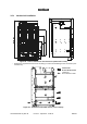
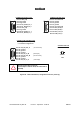
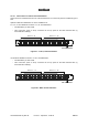
Figure 44 – DBS connections, assignment of access points (1)
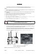
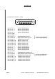
Do not connect pins 01 and 06
(clock output: 75 ohms load, 06 connected to
ground)
Pin 01: not connected
Pin 02: ground
Pin 03: ground
Pin 05: not connected
Pin 07: 10BT_RxD_P
Pin 08: 10BT_TxD_M
Pin 04: ground
Pin 06: 10BT_RxD_M
CONNECTOR NMS J102
Pin 01: SDA_Fdp
Pin 02: ground
Pin 03: ground
Pin 07: ground
Pin 08: PC_RS232_Tx_1
Pin 04: PC_RS232_Rx_1
Pin 06: SCL_Fdp
CONNECTOR TEST#1 J101
Pin 05: PC_RS232_Rx_0
Pin 09: PC_RS232_Tx_0
Pin 09: 10BT_TxD_P
Pin 01: Clk_2M_Out_P
Pin 02: ground
Pin 03: ground
Pin 05: Clk_2M_In_M
Pin 07: ground
Pin 08: ground
Pin 04: ground
Pin 06: Clk_2M_Out_M
Pin 09: Clk_2M_In_P
CONNECTOR SYNCHRO J103
(do not connect)
(do not connect)
TEST#2
J1
13
CONNECTOR J1
13
DO NOT CONNECT
Clock signals have no polarity
––
> P and M not significant
(clock input)
(clock input)