
Technical data
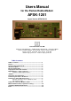

AFSK1201 Seite 3
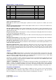
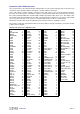
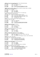
Digital interface - 20 pin connector
Pin Signal Function Pin Signal
1 + 5 Volt power supply 5 volt 150 mA (from TNC) 2 Ground
3 + 5 Volt power supply 5 volt 150 mA (from TNC) 4 Ground
5 Reset (not used in FSK9600) 6 Ground
7 DCD AF carrier detect (from modem to TNC) 8 Ground
9 CTS transmitter is keyed (from modem to TNC) 10 Ground
11 PTT transmitter keying (from TNC to modem) 12 Ground
13 TXD transmit data (from TNC to modem) 14 Ground
15 RXD* receive data (from modem to TNC) 16 Ground
17 TXC transmit clock (from modem to TNC) 18 Ground
19 RXC* receive clock (from modem to TNC) 20 Ground
*: RXD and TXD can be encoded NRZ as well as NRZI.
Signal description digital interface
Reset (pin 5): (modem input) normally high, is pulled low for 50 ms at power-on of TNC3. (not used in
FSK1201)
DCD (pin 7) Data Carrier Detect: (modem output) High: modem receives no carrier, low: modem has de-
tected a 1200 baud AFSK signal.
CTS (pin 9) Clear to Send: (modem output) Normally high. If the modem is ready to transmit data, the sig-
nal is low. With the FSK1200, CTS output is connected to PTT input. The TNC will wait for CTS=low before
data transmission starts.
PTT (pin 11) Push to talk, or RTS (Request to send): (modem input) normally high. When the transmitter is
to be keyed, the TNC pulls this signal to low.
TXD (pin 13) Transmit Data: (modem input): The data is latched at rising edge (low to high transition) of
transmit clock.
RXD (pin 15) Receive Data: (modem output): The data output changes at the falling edge and is valid at the
rising edge (low to high transition) of the receive clock.
TXC (pin 17) Transmit Clock: (modem output): The modem generates a clock frequency, which determines
the transmit baudrate and the data speed between TNC and modem. Transmit data signal TXD has to be
stable at the rising edge of TXC.
RXC (pin 19) Receive Clock: (modem output): the output of the receive clock recovery circuit is sent to the
TNC to synchronise the received data signal. RXD is stable at the rising edge of RXC. The frequency of
RXC corresponds to the transmit clock of the remote transmitter. If the internal clock of the modem and the
clock of the remote transmitter differ by some percent, the receive clock is adjusted by 1/16 clock cycle to
maintain synchronism.
Jumpers
Jumper J1 / J2 "DCD": AFSK-1201 has a carrier detect circuit using the XT2211 tone decoder. This circuit
is called Ädigital squelch' (however this expression isn't correct at all as the tone detection uses analog IC
only). The modem is shipped with the jumper set to XR2211-DCD, the channel is busy if a audio signal
within the normal bandwidth of a packet-radio signal is detected.
Sometimes it is desirable to define a channel to be busy if there is any audio frequency signal present (even
noise). If you prefer this, you can disconnect the XR2211 carrier detect and use the TCM3105 cattier detect
circuitry. Open the jumper J1 and close J2.
Jumper J3 "WATCHDOG": There is a time-limit for keying the transmitter. If the transwith time of approx.
40-50s is expired, the transmitter keying is released even when the controlling TNC keeps the PTT line
LOW. So, it is made sure that the transmitter never 'hangs'. This kind of protection circuit is called Watchdog.
For full duplex applications or digipeaters the watchdog may be disabled by installing a solder jumper to J3.
Test points and adjustment
Test point MP1 "DCD": The carrier detect with the ic XR2211 has to be set to the correct center frequency
by adjusting trimmer P 2. Watch the voltage at MP1 (oscilloscope) and adjust for best 1:1 duty cycle (HI:LO
ratio). The signal looks like a half way rectified sinewave, the adjustment is not critical.