User's Guide http://www.omega.com e-mail: info@omega.
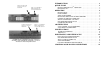
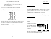
C a ble fro m D IO bo ard plu gs into co n n ecto r lab ele d IN INTRODUCTION QUICK START C a ble to seco nd E R B o r S S R b oa rd plu gs in to co nn ecto r la be led O U T C a ble fro m D IO bo ard plu gs into co n n ecto r lab ele d IN C a ble to seco nd E R B o r S S R b oa rd plu gs in to co nn ecto r la be led O U T C IO -ER B -24 and SS R -R A C K 24 pro vide co nnectors allo w ing a sing le C IO -D IO -48 style bo ard to con tro l o r m o n itor tw o 24-bit relay/SS R b o ards . .............
INTRODUCTION This manual provides complete information on CIO-DIO48, CIO-DIO48H, CIODIO96 and CIO-DIO192 digital I/O boards and accessories. The manual is organized into separate sections for those aspects of a product which are unique. Some issues, such as BASIC programming and electronic interfacing are applicable to all of the digital boards. The CIO-DIO48 has two 82C55 parallel interface chips and a 50 pin connector. Each 82C55 controls 24 CMOS/TTLcompatible digital I/O pins.
QUICK START LOW PASS FILTERS DE-BOUNCE INPUTS A low pass filter is placed on the signal wires between a signal and an A/D board. It stops frequencies greater than the cut off frequency from entering the A/D board's analog or digital inputs. The key term in a low pass filter circuit is cut off frequency. The cut of frequency is that frequency above which no variation of voltage with respect to time may enter the circuit.
2. Select Board #0 (select another number if Board #0 is already installed) Attenuation = R1 + R2 R2 3. Select Board Type 4. Move through the selections and highlight the particular board you are installing (e.g. CIO-DIO48H or CIO-DIO192). Either double click on the board or hit enter. 2 = 10K + 10K 10K 5. The board’s default settings are then displayed. The board’s defaults are: BASE ADDRESS: WAIT STATE: 300H (768 Decimal) Same as data sheet. OFF. 6.
Voltage = Current * Resistance (commonly V=IR) OPERATION and Kirkoff's voltage law which states, The sum of the voltage drops around a circuit will be equal to the voltage drop for the entire circuit. Implied in the above is that any variation in the voltage drop for the circuit as a whole will have a proportional variation in all the voltage drops in the circuit.
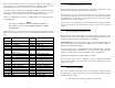
The base address switch is the means for setting the base address. Each switch position corresponds to one of the PC bus address lines. By placing the switch down, the CIO-DIO address decode logic is instructed to respond to that address bit. A complete address is constructed by calculating the HEX or decimal number which corresponds to all the address bits the CIO-DIO has been instructed to respond to. For example, shown to the right are address 9 and 8 DOWN, all others UP.
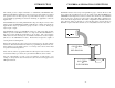
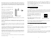
If the inputs of the device you are controlling are left to float, they may float up or down. Which way they float is dependent on the characteristics of the circuit and the electrical environment; and unpredictable! This is why it often appears that the 82C55 has gone 'high' after power up. The result is that your controlled device gets turned on! That is why you need pull up/down resistors. Shown here is one 82C55 digital output with a pull-up resistor attached.
CABLING TO THE DIO CONNECTOR The CIO-DIO48 connector is accessible through the PC/AT expansion bracket. The connector is a standard 50 pin male header connector. A mating female connector may be purchased at Radio Shack or other electronic supply outlets. SIGNAL CONNECTION - CIO-DIO48 All the digital outputs and inputs on the CIO-DIO48 connector are CMOS/TTL.
DIGITAL I/O UNCONNECTED INPUTS FLOAT TTL LEVEL DIRECT TO/FROM 82C55 Keep in mind that unconnected inputs float. If you are using a DIO board for input, and have unconnected inputs, ignore the data from those lines. 82C55 output high 3.0 V min @ -2.5Ma 82C55 output low0.4 V max @ 2.5 mA 82C55 input high 2.0 V min, 7 V max 82C55 input low -0.5 V min, 0.8 V max 82C55 drive capability 5 LSTTL loads HIGH DRIVE DIO48H Output High Output Low Input High Input Low 2.0V min @ -15mA 0.55V max @ 64mA 2.0V min, 7.
ARCHITECTURE 82C55 CONTROL & DATA REGISTERS POWER CONSUMPTION Each CIO-DIO is composed of 82C55 parallel I/O chips. Each chip contains 3 data and one control register occupying 4 consecutive I/O locations. The number of I/O locations occupied by a CIO-DIO board is equal to 4 times the number of 82C55 chips on the board. The first address, or BASE ADDRESS, is determined by setting a bank of switches on the board. A register is easy to read and write to.
The two groups of ports, group A and group B, may be independently programmed in one of several modes. The most commonly used mode is mode 0, input / output mode. The codes for programming the 82C55 in this mode are shown below. D7 is always 1 and D6, D5 & D2 are always 0.
In 82C55 mode 0 configuration, ports configured for output hold the output data written. The output byte may be read back by reading a port configured for output. 82C55 DIGITAL I/O REGISTERS PORT A DATA BASE ADDRESS +0 7 6 A7 A6 5 A5 4 A4 3 A3 2 A2 1 A1 0 A0 PORT B DATA BASE ADDRESS +1 7 6 B7 B6 5 B5 4 B4 3 B3 2 B2 1 B1 0 B0 Ports A & B may be programmed as input or output.