
Datasheet


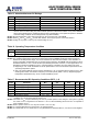


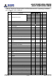


Table 15. Absolute Maximum DC Ratings
Symbol
Parameter
Values
Unit
Note
V
DD
Voltage on VDD pin relative to Vss
-1.0 ~ 2.3
V
1,3
V
DDQ
Voltage on VDDQ pin relative to Vss
-0.5 ~ 2.3
V
1,3
V
DDL
Voltage on VDDL pin relative to Vss
-0.5 ~ 2.3
V
1,3
V
IN
, V
OUT
Voltage on any pin relative to Vss
-0.5 ~ 2.3
V
1,4
T
STG
Storage temperature
-55 ~ 100
∞
C
1,2
NOTE1: Stress greater than those listed under “Absolute Maximum Ratings” may cause permanent damage to the
devices. This is a stress rating only and functional operation of the device at these or any other conditions
above those indicated in the operational sections of this specification is not implied. Exposure to absolute
maximum rating conditions for extended periods may affect reliability.
NOTE2: Storage temperature is the case temperature on the center/top side of the DRAM.
NOTE3: When V
DD
and V
DDQ
and V
DDL
are less than 500mV, Vref may be equal to or less than 300mV.
NOTE4: Voltage on any input or I/O may not exceed voltage on V
DDQ.
T
able 16. Operating Temperature Condition
Symbol
Parameter
Values
Unit
Note
T
OPER
Commercial temperature
0 ~ 85
°
C
1,2
Industrial temperature
-40 ~ 95
°
C
1,2
NOTE1: Operating Temperature is the case surface temperature on the center/top side of the DRAM.
NOTE2: The operation temperature range are the temperature where all DRAM specification will be supported.
Outside of this temperature range, even if it is still within the limit of stress condition, some deviation on
portion of operation specification may be required. During operation, the DRAM case temperature must be
maintained between 0 - 85 °C under all other specification parameter. However, in some applications, it is
desirable to operate the DRAM up to 95 °C case temperature. Therefore, two spec options may exist.
a) Supporting 0 - 85 °C with full JEDEC AC & DC specifications. This is the minimum requirements for all
operating temperature options.
b) This is an optional feature and not required. Supporting 0 - 85 °C and being able to extend to 95 °C with
doubling auto-refresh commands in frequency to a 32 ms period ( tREFI = 3.9 us). Supporting higher
temperature Self-Refresh entry via the control of EMSR (2) bit A7.
Table 17. Recommended DC Operating Conditions (SSTL_1.8)
Symbol
Parameter
Min.
Typ.
Max.
Unit
Note
V
DD
Power supply voltage
1.7
1.8
1.9
V
1
V
DDL
Power supply voltage for DLL
1.7
1.8
1.9
V
5
V
DDQ
Power supply voltage for I/O Buffer
1.7
1.8
1.9
V
1,5
V
REF
Input reference voltage
0.49 x V
DDQ
0.5 x V
DDQ
0.51 x V
DDQ
mV
2,3
V
TT
Termination voltage
V
REF
- 0.04
V
REF
V
REF
+ 0.04
V
4
NOTE1: There is no specific device VDD supply voltage requirement for SSTL_18 compliance. However under all
conditions V
DDQ
must be less than or equal to V
DD.
NOTE2: The value of V
REF
may be selected by the user to provide optimum noise margin in the system. Typically
the value of V
REF
is expected to be about 0.5 x V
DDQ
of the transmitting device and V
REF
is expected to
track variations in V
DDQ
.
NOTE3: Peak to peak ac noise on V
REF
may not exceed +/-2 % V
REF
(dc).
NOTE4: V
TT
of transmitting device must track V
REF
of receiving device.
NOTE5: V
DDQ
tracks with V
DD
, V
DDL
tracks with V
DD
. AC parameters are measured with V
DD
, V
DDQ
and V
DDL
tied together.
AS4C128M16D2A-25BCN
AS4C128M16D2A-25BIN
Confidential
- 23/63 -
Rev.1.0 Dec 2015