
Instruction manual
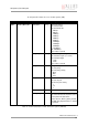
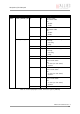
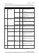
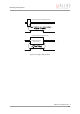
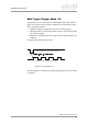

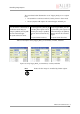
Table Of Contents
- Introduction
- Declarations of conformity
- Safety instructions
- PIKE types and highlights
- FireWire
- Overview
- FireWire in detail
- Serial bus
- FireWire connection capabilities
- Capabilities of 1394a (FireWire 400)
- Capabilities of 1394b (FireWire 800)
- Compatibility between 1394a and 1394b
- Image transfer via 1394a and 1394b
- 1394b bandwidths
- FireWire Plug & play capabilities
- FireWire hot plug precautions
- Operating system support
- 1394a/b comparison
- System components
- Specifications
- Camera dimensions
- PIKE standard housing (2 x 1394b copper)
- PIKE (1394b: 1 x GOF, 1 x copper)
- Tripod adapter
- Pike W90 (2 x 1394b copper)
- Pike W90 (1394b: 1 x GOF, 1 x copper)
- Pike W90 S90 (2 x 1394b copper)
- Pike W90 S90 (1394b: 1 x GOF, 1 x copper)
- Pike W270 (2 x 1394b copper)
- Pike W270 (1394b: 1 x GOF, 1 x copper)
- Pike W270 S90 (2 x 1394b copper)
- Pike W270 S90 (1394b: 1 x GOF, 1 x copper)
- Cross section: C-Mount (VGA size filter)
- Cross section: C-Mount (large filter)
- Adjustment of C-Mount
- F-Mount, K-Mount, M39-Mount
- Camera interfaces
- Description of the data path
- Block diagrams of the cameras
- Sensor
- Channel balance
- White balance
- Auto shutter
- Auto gain
- Manual gain
- Brightness (black level or offset)
- Horizontal mirror function
- Shading correction
- Look-up table (LUT) and gamma function
- Binning (b/w models)
- Sub-sampling
- High SNR mode (High Signal Noise Ratio)
- Frame memory and deferred image transport
- Color interpolation (BAYER demosaicing)
- Sharpness
- Hue and saturation
- Color correction
- Color conversion (RGB ‡ YUV)
- Bulk Trigger
- Level Trigger
- Serial interface
- Controlling image capture
- Video formats, modes and bandwidth
- How does bandwidth affect the frame rate?
- Configuration of the camera
- Camera_Status_Register
- Configuration ROM
- Implemented registers
- Camera initialize register
- Inquiry register for video format
- Inquiry register for video mode
- Inquiry register for video frame rate and base address
- Inquiry register for basic function
- Inquiry register for feature presence
- Inquiry register for feature elements
- Inquiry register for absolute value CSR offset address
- Status and control register for feature
- Feature control error status register
- Video mode control and status registers for Format_7
- Advanced features
- Version information inquiry
- Advanced feature inquiry
- Camera status
- Maximum resolution
- Time base
- Extended shutter
- Test images
- Look-up tables (LUT)
- Shading correction
- Deferred image transport
- Frame information
- Input/output pin control
- Delayed Integration enable
- Auto shutter control
- Auto gain control
- Autofunction AOI
- Color correction
- Trigger delay
- Mirror image
- AFE channel compensation (channel balance)
- Soft Reset
- High SNR mode (High Signal Noise Ratio)
- User profiles
- GPDATA_BUFFER
- Firmware update
- Glossary
- Index

Description of the data path
PIKE Technical Manual V3.1.0
143
008h RECEIVE_BUFFER_
STATUS_CONTRL
RBUF_ST [0..7] SIO receive buffer status
RD: Number of bytes pending in receive
buffer
WR: Ignored
RBUF_CNT [8..15] SIO receive buffer control
RD: Number of bytes to be read from the
receive FiFo
WR: Number of bytes left for readout
from the receive FiFo
- [16..31] Reserved
00Ch TRANSMIT_BUFFER_
STATUS_CONTRL
TBUF_ST [0..7] SIO output buffer status
RD: Space left in TX buffer
WR: Ignored
TBUF_CNT [8..15] SIO output buffer control
RD: Number of bytes written to transmit
FiFo
WR: Number of bytes to transmit
- [16..31] Reserved
010h
..
0FFh
- Reserved
100h SIO_DATA_REGISTER CHAR_0 [0..7] Character_0
RD: Read character from receive buffer
WR: Write character to transmit buffer
SIO_DATA_REGISTER CHAR_1 [8..15] Character_1
RD: Read character from receive
buffer+1
WR: Write character to transmit
buffer+1
SIO_DATA_REGISTER CHAR_2 [16..23] Character_2
RD: Read character from receive
buffer+2
WR: Write character to transmit
buffer+2
SIO_DATA_REGISTER CHAR_3 [24..31] Character_3
RD: Read character from receive
buffer+3
WR: Write character to transmit
buffer+3
104h
..
1FFH
SIO_DATA_REGISTER_
ALIAS
[0..31] Alias SIO_Data_Register area for block
transfer
Offset Name Field Bit Description
Table 54: Serial input/output control and status register (SIO CSR)