
Instruction manual

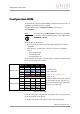
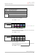
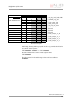


Table Of Contents
- Introduction
- Declarations of conformity
- Safety instructions
- PIKE types and highlights
- FireWire
- Overview
- FireWire in detail
- Serial bus
- FireWire connection capabilities
- Capabilities of 1394a (FireWire 400)
- Capabilities of 1394b (FireWire 800)
- Compatibility between 1394a and 1394b
- Image transfer via 1394a and 1394b
- 1394b bandwidths
- FireWire Plug & play capabilities
- FireWire hot plug precautions
- Operating system support
- 1394a/b comparison
- System components
- Specifications
- Camera dimensions
- PIKE standard housing (2 x 1394b copper)
- PIKE (1394b: 1 x GOF, 1 x copper)
- Tripod adapter
- Pike W90 (2 x 1394b copper)
- Pike W90 (1394b: 1 x GOF, 1 x copper)
- Pike W90 S90 (2 x 1394b copper)
- Pike W90 S90 (1394b: 1 x GOF, 1 x copper)
- Pike W270 (2 x 1394b copper)
- Pike W270 (1394b: 1 x GOF, 1 x copper)
- Pike W270 S90 (2 x 1394b copper)
- Pike W270 S90 (1394b: 1 x GOF, 1 x copper)
- Cross section: C-Mount (VGA size filter)
- Cross section: C-Mount (large filter)
- Adjustment of C-Mount
- F-Mount, K-Mount, M39-Mount
- Camera interfaces
- Description of the data path
- Block diagrams of the cameras
- Sensor
- Channel balance
- White balance
- Auto shutter
- Auto gain
- Manual gain
- Brightness (black level or offset)
- Horizontal mirror function
- Shading correction
- Look-up table (LUT) and gamma function
- Binning (b/w models)
- Sub-sampling
- High SNR mode (High Signal Noise Ratio)
- Frame memory and deferred image transport
- Color interpolation (BAYER demosaicing)
- Sharpness
- Hue and saturation
- Color correction
- Color conversion (RGB ‡ YUV)
- Bulk Trigger
- Level Trigger
- Serial interface
- Controlling image capture
- Video formats, modes and bandwidth
- How does bandwidth affect the frame rate?
- Configuration of the camera
- Camera_Status_Register
- Configuration ROM
- Implemented registers
- Camera initialize register
- Inquiry register for video format
- Inquiry register for video mode
- Inquiry register for video frame rate and base address
- Inquiry register for basic function
- Inquiry register for feature presence
- Inquiry register for feature elements
- Inquiry register for absolute value CSR offset address
- Status and control register for feature
- Feature control error status register
- Video mode control and status registers for Format_7
- Advanced features
- Version information inquiry
- Advanced feature inquiry
- Camera status
- Maximum resolution
- Time base
- Extended shutter
- Test images
- Look-up tables (LUT)
- Shading correction
- Deferred image transport
- Frame information
- Input/output pin control
- Delayed Integration enable
- Auto shutter control
- Auto gain control
- Autofunction AOI
- Color correction
- Trigger delay
- Mirror image
- AFE channel compensation (channel balance)
- Soft Reset
- High SNR mode (High Signal Noise Ratio)
- User profiles
- GPDATA_BUFFER
- Firmware update
- Glossary
- Index

Configuration of the camera
PIKE Technical Manual V3.1.0
192
Configuration ROM
The information in the Configuration ROM is needed to identify the node, its
capabilities and which drivers are required.
The base address for the configuration ROM for all registers is
FFFF F0000000h.
The ConfigRom is divided into
• Bus info block: providing critical information about the bus-related
capabilities
• Root directory: specifying the rest of the content and organization,
such as:
– Node unique ID leaf
– Unit directory and
–Unit dependant info
The base address of the camera control register is calculated as follows based
on the camera-specific base address:
The entry with key 8D in the root directory (420h in this case) provides the
offset for the Node unique ID leaf.
To compute the effective start address of the node unique ID leaf:
Note
L
If you want to use the DirectControl program to read or write
to a register, enter the following value in the Address field:
F0F00000h + Offset
Bus info block
Offset 0-7 8-15 16-23 24-31
400h 04 29 0C C0
404h
31 33 39 34 …. ASCII for 1394
408h 20 00 B2 03 …. Bus capabilities
40Ch
00 0A 47 01 …. Node_Vendor_Id, Chip_id_hi
410h
Serial number …. Chip_id_lo
Root directory
414h 00 04 B7 85 According to IEEE1212, the root directory
may have another length. The keys (e.g.
8D) point to the offset factors rather than
the offset (e.g. 420h) itself.
418h 03 00 0A 47
41Ch 0C 00 83 C0
420h
8D 00 00 02
424h
D1 00 00 04
Table 92: Config ROM